SLVSFQ6A November   2020  – June 2021 TPS2640

PRODUCTION DATA  

  1. Features
  2. Applications
  3. Description
  4. Revision History
  5. Device Comparison
  6. Pin Configuration and Functions
  7. Specifications
    1. 7.1 Absolute Maximum Ratings
    2. 7.2 ESD Ratings
    3. 7.3 Recommended Operating Conditions
    4. 7.4 Thermal Information
    5. 7.5 Electrical Characteristics
    6. 7.6 Timing Requirements
    7. 7.7 Typical Characteristics
  8. Parameter Measurement Information
  9. Detailed Description
    1. 9.1 Overview
    2. 9.2 Functional Block Diagram
    3. 9.3 Feature Description
      1. 9.3.1 Undervoltage Lockout (UVLO)
      2. 9.3.2 Overvoltage Protection (OVP)
      3. 9.3.3 Reverse Input Supply Protection
      4. 9.3.4 Hot Plug-In and In-Rush Current Control
      5. 9.3.5 Overload and Short Circuit Protection
        1. 9.3.5.1 Overload Protection
          1. 9.3.5.1.1 Active Current Limiting
          2. 9.3.5.1.2 Electronic Circuit Breaker with Overload Timeout, MODE = OPEN
        2. 9.3.5.2 Short Circuit Protection
          1. 9.3.5.2.1 Start-Up With Short-Circuit On Output
        3. 9.3.5.3 FAULT Response
          1. 9.3.5.3.1 Look Ahead Overload Current Fault Indicator
        4. 9.3.5.4 Current Monitoring
        5. 9.3.5.5 IN, OUT, RTN, and GND Pins
        6. 9.3.5.6 Thermal Shutdown
        7. 9.3.5.7 Low Current Shutdown Control (SHDN)
    4. 9.4 Device Functional Modes
  10. 10Application and Implementation
    1. 10.1 Application Information
    2. 10.2 Typical Application
      1. 10.2.1 Design Requirements
      2. 10.2.2 Detailed Design Procedure
        1. 10.2.2.1 Step by Step Design Procedure
        2. 10.2.2.2 Undervoltage Lockout and Overvoltage Set Point
        3. 10.2.2.3 Programming Current Monitoring Resistor—RIMON
        4. 10.2.2.4 Setting Output Voltage Ramp Time—(tdVdT)
          1. 10.2.2.4.1 Case 1: Start-Up Without Load—Only Output Capacitance C(OUT) Draws Current During Start-Up
          2. 10.2.2.4.2 Case 2: Start-Up With Load—Output Capacitance C(OUT) and Load Draws Current During Start-Up
          3. 10.2.2.4.3 Support Component Selections—RFLTb and C(IN)
      3. 10.2.3 Application Curves
    3. 10.3 System Examples
      1. 10.3.1 Acive ORing Operation
      2. 10.3.2 Field Supply Protection in PLC, DCS I/O Modules
      3. 10.3.3 Simple 24-V Power Supply Path Protection
    4. 10.4 Do's and Dont's
  11. 11Power Supply Recommendations
    1. 11.1 Transient Protection
  12. 12Layout
    1. 12.1 Layout Guidelines
    2. 12.2 Layout Example
  13. 13Device and Documentation Support
    1. 13.1 Device Support
    2. 13.2 Documentation Support
      1. 13.2.1 Related Documentation
    3. 13.3 Receiving Notification of Documentation Updates
    4. 13.4 Support Resources
    5. 13.5 Trademarks
    6. 13.6 Electrostatic Discharge Caution
    7. 13.7 Glossary
  14. 14Mechanical, Packaging, and Orderable Information

Package Options

Mechanical Data (Package|Pins)
Thermal pad, mechanical data (Package|Pins)
Orderable Information

Current Monitoring

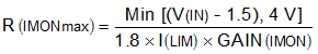
The current source at IMON terminal is internally configured to be proportional to the current flowing from IN to OUT. This current can be converted into a voltage using a resistor R(IMON) from IMON terminal to RTN terminal. The IMON voltage can be used as a means of monitoring current flow through the system. The maximum voltage range (V(IMONmax)) for monitoring the current is limited to minimum of ([V(IN) – 1.5 V, 4 V]) to ensure linear output. This puts a limitation on maximum value of R(IMON) resistor and is determined by Equation 5.

Equation 5. GUID-20200603-SS0I-2SMT-HRNV-KBTGQPD6PKWJ-low.gif

The output voltage at IMON terminal is calculated using Equation 6 and Equation 7.

For IOUT > 50 mA,

Equation 6. V(IMON) = [I(OUT) × GAIN(IMON)] × R(IMON)

where,

  • GAIN(IMON) is the gain factor I(IMON):I(OUT) = 78.4 μA/A (Typical)
  • I(OUT) is the load current
  • I(MON_OS) = 2 μA (Typical)

For IOUT < 50 mA (typical), use Equation 7.

Equation 7. V(IMON) = (I(IMON_ OS)) × R(IMON)

This pin must not have a bypass capacitor to avoid delay in the current monitoring information. In case of reverse input polarity fault, an external 100-kΩ resistor is recommended between IMON pin and ADC input to limit the current through the ESD protection structures of the ADC.