SLVSD88L July 2016 – August 2021 TPS61099
PRODUCTION DATA
- 1 Features
- 2 Applications
- 3 Description
- 4 Revision History
- 5 Device Comparison Table
- 6 Pin Configuration and Functions
- 7 Specifications
- 8 Detailed Description
- 9 Application and Implementation
- 10Power Supply Recommendations
- 11Layout
- 12Device and Documentation Support
- 13Mechanical, Packaging, and Orderable Information
Package Options
Mechanical Data (Package|Pins)
Thermal pad, mechanical data (Package|Pins)
- DRV|6
Orderable Information
8.3.8 Down Mode Regulation and Pass-Through Operation
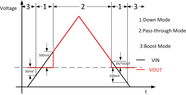
The TPS61099x features Down Mode and Pass-Through operation when input voltage is close to or higher than output voltage.
In the Down Mode, output voltage is regulated at target value even when VIN > VOUT. The control circuit changes the behavior of the rectifying PMOS by pulling its gate to input voltage instead of to ground. In this way, the voltage drop across the PMOS is increasing as high as to regulate the output voltage. The power loss also increases in this mode, which needs to be taken into account for thermal consideration.
In the Pass-Through operation, the boost converter stops switching. The rectifying PMOS constantly turns on and low side switch constantly turns off. The output voltage is the input voltage minus the voltage drop across the dc resistance (DCR) of the inductor and the on-resistance of the rectifying PMOS.
With VIN ramping up, the TPS61099x goes into Down Mode first when VIN > VOUT – 50mV. It stays in Down Mode until VIN > VOUT + 0.5 V and then goes automatically into Pass-Through operation. In the Pass-Through operation, output voltage follows input voltage. The TPS61099x exits Pass-Through Mode and goes back to Down Mode when VIN ramps down to 103% of the target output voltage. It stays in Down Mode until input voltage falls 100mV below the output voltage, returning to Boost operation.
 Figure 8-4 Down Mode and Pass-Through Operation