SLVSFS7A March 2021 – January 2024 TPS62901
PRODUCTION DATA
- 1
- 1 Features
- 2 Applications
- 3 Description
- 4 Pin Configuration and Functions
- 5 Specifications
-
6 Detailed Description
- 6.1 Overview
- 6.2 Functional Block Diagram
- 6.3
Feature Description
- 6.3.1 Mode Selection and Device Configuration MODE/S-CONF
- 6.3.2 Adjustable VO Operation (External Voltage Divider)
- 6.3.3 Setable VO Operation (VSET and Internal Voltage Divider)
- 6.3.4 Soft Start / Tracking (SS/TR)
- 6.3.5 Smart Enable with Precise Threshold
- 6.3.6 Power Good (PG)
- 6.3.7 Undervoltage Lockout (UVLO)
- 6.3.8 Current Limit And Short-Circuit Protection
- 6.3.9 Thermal Shutdown
- 6.4 Device Functional Modes
-
7 Application and Implementation
- 7.1 Application Information
- 7.2
Typical Application with Adjustable Output Voltage
- 7.2.1 Design Requirements
- 7.2.2 Detailed Design Procedure
- 7.2.3 Application Curves
- 7.2.4 Typical Application with Setable VO using VSET
- 7.3 System Examples
- 7.4 Power Supply Recommendations
- 7.5 Layout
- 8 Device and Documentation Support
- 9 Revision History
- 10Mechanical, Packaging, and Orderable Information
Package Options
Mechanical Data (Package|Pins)
- RPJ|9
Thermal pad, mechanical data (Package|Pins)
Orderable Information
6.4.3 Power Save Mode Operation (Auto PFM/PWM)
When the MODE/S-CONF pin is configured for power save mode (auto PFM/PWM). The device operates in PWM mode as long the output current is higher than half of the ripple current of the inductor. To maintain high efficiency at light loads, the device enters power save mode at the boundary to discontinuous conduction mode (DCM). This happens if the output current becomes smaller than half of the ripple current of the inductor. The power save mode is entered seamlessly when the load current decreases. This ensures a high efficiency in light load operation. The device remains in power save mode as long as the inductor current is discontinuous.
In power save mode, the switching frequency decreases linearly with the load current maintaining high efficiency. The transition in and out of power save mode is seamless in both directions.
In addition to adjusting the switching, the TPS62901 adjusts the on-time (TON) in power save mode, depending on the input voltage and the output voltage to maintain highest efficiency using the AEE function when 2.5MHz is selected as described in Section 6.4.2.
In power save mode, the TON time can be estimated using Equation 3 for 1MHz and Equation 5 for 2.5MHz (given the AEE is enabled for 2.5MHz).
For very small output voltages, an absolute minimum on-time of about 50ns is kept to limit switching losses. The operating frequency is thereby reduced from the nominal value, which keeps efficiency high. Using TON, the typical peak inductor current in power save mode is approximated by Equation 7:

There is a minimum off-time which limits the duty cycle of the TPS62901. When VIN decreases to typically 15% above VOUT, the TPS62901 does not enter power save mode, regardless of the load current. The device maintains output regulation in PWM mode.
The output voltage ripple in power save mode is given by Equation 8:
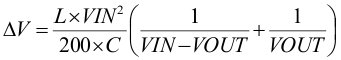
where
- L is the effective inductance
- C is the output effective capacitance