SLVSFS7A March 2021 – January 2024 TPS62901
PRODUCTION DATA
- 1
- 1 Features
- 2 Applications
- 3 Description
- 4 Pin Configuration and Functions
- 5 Specifications
-
6 Detailed Description
- 6.1 Overview
- 6.2 Functional Block Diagram
- 6.3
Feature Description
- 6.3.1 Mode Selection and Device Configuration MODE/S-CONF
- 6.3.2 Adjustable VO Operation (External Voltage Divider)
- 6.3.3 Setable VO Operation (VSET and Internal Voltage Divider)
- 6.3.4 Soft Start / Tracking (SS/TR)
- 6.3.5 Smart Enable with Precise Threshold
- 6.3.6 Power Good (PG)
- 6.3.7 Undervoltage Lockout (UVLO)
- 6.3.8 Current Limit And Short-Circuit Protection
- 6.3.9 Thermal Shutdown
- 6.4 Device Functional Modes
-
7 Application and Implementation
- 7.1 Application Information
- 7.2
Typical Application with Adjustable Output Voltage
- 7.2.1 Design Requirements
- 7.2.2 Detailed Design Procedure
- 7.2.3 Application Curves
- 7.2.4 Typical Application with Setable VO using VSET
- 7.3 System Examples
- 7.4 Power Supply Recommendations
- 7.5 Layout
- 8 Device and Documentation Support
- 9 Revision History
- 10Mechanical, Packaging, and Orderable Information
Package Options
Mechanical Data (Package|Pins)
- RPJ|9
Thermal pad, mechanical data (Package|Pins)
Orderable Information
7.3.1 LED Power Supply
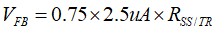
The TPS62901 can be used as a power supply for power LEDs. The FB pin can be easily set to lower values than nominal by using the SS/TR pin. With that, the voltage drop on the sense resistor is low to avoid excessive power loss. Because this pin provides 2.5µA, the feedback pin voltage can be adjusted by an external resistor per Equation 21. This drop, proportional to the LED current, is used to regulate the output voltage (anode voltage) to a proper level to drive the LED. Both analog and PWM dimming are supported with the TPS62901. Figure 7-81 shows an application circuit, tested with analog dimming.
 Figure 7-81 Single Power LED
Supply
Figure 7-81 Single Power LED
SupplyThe resistor at SS/TR defines the FB voltage. It is set to 304mV by RSS/TR = R4 = 162kΩ using Equation 21. This cuts the losses on R4 to half from the nominal 0.6V of feedback voltage while it still provides good accuracy.
The device now supplies a constant current set by resistor R2 from FB/VSET to GND. The minimum input voltage has to be rated according the forward voltage needed by the LED used. More information is available in SLVA451.