SLVSF29C October 2019 – August 2021 TPS8804
PRODUCTION DATA
- 1 Features
- 2 Applications
- 3 Description
- 4 Revision History
- 5 Pin Configuration and Functions
- 6 Specifications
-
7 Detailed Description
- 7.1 Overview
- 7.2 Functional Block Diagram
- 7.3 Feature Description
- 7.4 Device Functional Modes
- 7.5 Programming
- 7.6
Register Maps
- 7.6.1 REVID Register (Offset = 0h) [reset = 0h]
- 7.6.2 STATUS1 Register (Offset = 1h) [reset = 0h]
- 7.6.3 STATUS2 Register (Offset = 2h) [reset = 0h]
- 7.6.4 MASK Register (Offset = 3h) [reset = 0h]
- 7.6.5 CONFIG1 Register (Offset = 4h) [reset = 20h]
- 7.6.6 CONFIG2 Register (Offset = 5h) [reset = 0h]
- 7.6.7 ENABLE1 Register (Offset = 6h) [reset = 0h]
- 7.6.8 ENABLE2 Register (Offset = 7h) [reset = 0h]
- 7.6.9 CONTROL Register (Offset = 8h) [reset = 0h]
- 7.6.10 GPIO_AMUX Register (Offset = Bh) [reset = 0h]
- 7.6.11 COSW Register (Offset = Ch) [reset = 0h]
- 7.6.12 CO Register (Offset = Dh) [reset = 0h]
- 7.6.13 LEDLDO Register (Offset = Fh) [reset = 0h]
- 7.6.14 PH_CTRL Register (Offset = 10h) [reset = 0h]
- 7.6.15 LED_DAC_A Register (Offset = 11h) [reset = 0h]
- 7.6.16 LED_DAC_B Register (Offset = 12h) [reset = 0h]
- 8 Application and Implementation
- 9 Power Supply Recommendations
- 10Layout
- 11Device and Documentation Support
- 12Mechanical, Packaging, and Orderable Information
Package Options
Mechanical Data (Package|Pins)
- DCP|38
Thermal pad, mechanical data (Package|Pins)
- DCP|38
Orderable Information
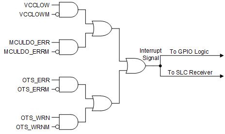
7.3.9 Interrupt Signal Alerts
 Figure 7-8 Interrupt Signal Alert Logic
Configurable interrupt signals notify the MCU when a system anomaly occurs. The interrupt signal indicates the STATUS1 register, which has bits that latch high when reaching various condition limits such as temperature or voltage. Each of the bits in the STATUS1 register can be independently configured to send an interrupt signal by setting the MASK register bit corresponding to each STATUS1 bit. The GPIO bits must be set to 0x2 to output interrupt signals through the GPIO pin, and the STATUS_MCURX bit must be set to 1 to output interrupt signals through the MCU_RX pin. By connecting the GPIO or MCU_RX pin to the microcontroller, the MCU can be immediately notified when a STATUS1 bit changes instead of having to repeatedly read the STATUS1 register. After the device sends the interrupt signal, the signal remains high until the STATUS1 register is read, at which point the fault clears if the error condition is removed.