SLVSF29C October 2019 – August 2021 TPS8804
PRODUCTION DATA
- 1 Features
- 2 Applications
- 3 Description
- 4 Revision History
- 5 Pin Configuration and Functions
- 6 Specifications
-
7 Detailed Description
- 7.1 Overview
- 7.2 Functional Block Diagram
- 7.3 Feature Description
- 7.4 Device Functional Modes
- 7.5 Programming
- 7.6
Register Maps
- 7.6.1 REVID Register (Offset = 0h) [reset = 0h]
- 7.6.2 STATUS1 Register (Offset = 1h) [reset = 0h]
- 7.6.3 STATUS2 Register (Offset = 2h) [reset = 0h]
- 7.6.4 MASK Register (Offset = 3h) [reset = 0h]
- 7.6.5 CONFIG1 Register (Offset = 4h) [reset = 20h]
- 7.6.6 CONFIG2 Register (Offset = 5h) [reset = 0h]
- 7.6.7 ENABLE1 Register (Offset = 6h) [reset = 0h]
- 7.6.8 ENABLE2 Register (Offset = 7h) [reset = 0h]
- 7.6.9 CONTROL Register (Offset = 8h) [reset = 0h]
- 7.6.10 GPIO_AMUX Register (Offset = Bh) [reset = 0h]
- 7.6.11 COSW Register (Offset = Ch) [reset = 0h]
- 7.6.12 CO Register (Offset = Dh) [reset = 0h]
- 7.6.13 LEDLDO Register (Offset = Fh) [reset = 0h]
- 7.6.14 PH_CTRL Register (Offset = 10h) [reset = 0h]
- 7.6.15 LED_DAC_A Register (Offset = 11h) [reset = 0h]
- 7.6.16 LED_DAC_B Register (Offset = 12h) [reset = 0h]
- 8 Application and Implementation
- 9 Power Supply Recommendations
- 10Layout
- 11Device and Documentation Support
- 12Mechanical, Packaging, and Orderable Information
Package Options
Mechanical Data (Package|Pins)
- DCP|38
Thermal pad, mechanical data (Package|Pins)
- DCP|38
Orderable Information
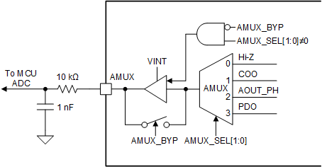
7.3.7 AMUX
 Figure 7-7 Analog Multiplexer Circuit
The AMUX switch and buffer are used to connect the various TPS8804 amplifier outputs to a single ADC. The unity-gain amplifier improves the drive strength and fidelity of the analog signals when connected to an ADC. A 330 pF to 1 nF capacitor must be connected to the AMUX pin to stabilize its output. The 10-kΩ resistor filters high-frequency noise in the analog signal. Using a 10-kΩ resistor and 1-nF capacitor reduces noise levels in the photo amplifier signal. The buffer has the option of being bypassed to remove the added offset introduced by the unity-gain amplifier. Because the AMUX requires the bias block (see Section 7.3.8), bypassing the buffer does not eliminate the AMUX current consumption.