SLUSD66D September 2019 – February 2021 TPS92520-Q1
PRODUCTION DATA
- 1 Features
- 2 Applications
- 3 Description
- 4 Revision History
- 5 Pin Configuration and Functions
- 6 Specifications
-
7 Detailed Description
- 7.1 Overview
- 7.2 Functional Block Diagram
- 7.3
Feature Description
- 7.3.1 Buck Converter Switching Operation
- 7.3.2 Switching Frequency and Adaptive On-Time Control
- 7.3.3 Minimum On-Time, Off-Time, and Inductor Ripple
- 7.3.4 LED Current Regulation and Error Amplifier
- 7.3.5 Start-up Sequence
- 7.3.6 Analog Dimming and Forced Continuous Conduction Mode
- 7.3.7 External PWM Dimming and Input Undervoltage Lockout (UVLO)
- 7.3.8 Internal PWM Dimming
- 7.3.9 Shunt FET Dimming or Matrix Beam Application
- 7.3.10 Bias Supply
- 7.3.11 Bootstrap Supply
- 7.3.12 ADC
- 7.3.13 Faults and Diagnostics
- 7.3.14 Output Short Circuit Fault
- 7.3.15 Output Open Circuit Fault
- 7.4 Device Functional Modes
- 7.5 Programming
- 7.6
Register Maps
- 7.6.1 Configuration Registers
- 7.6.2 STATUS Registers
- 7.6.3
Device Control Registers
- 7.6.3.1 Thermal Warning Limit (address = 0x06) [reset = 0x8A]
- 7.6.3.2 SLEEP Command (address = 0x07) [reset = 0x00]
- 7.6.3.3 CH1IADJL Control Register (address = 0x08) [reset = 0x00]
- 7.6.3.4 CH1IADJH Control Register (address = 0x09) [reset = 0x00]
- 7.6.3.5 CH2IADJL Control Register (address = 0x0A) [reset = 0x00]
- 7.6.3.6 CH2IADJH Control Register (address = 0x0B) [reset = 0x00]
- 7.6.3.7 PWMDIV Register (address = 0x0C) [reset = 0x04]
- 7.6.3.8 CH1PWML Register (address = 0x0D) [reset = 0x00]
- 7.6.3.9 CH1PWMH Register (address = 0x0E) [reset = 0x00]
- 7.6.3.10 CH2PWML Register (address = 0x0F) [reset = 0x00]
- 7.6.3.11 CH2PWMH Register (address = 0x10) [reset = 0x00]
- 7.6.3.12 CH1TON Register (address = 0x11) [reset = 0x07]
- 7.6.3.13 CH2TON Register (address = 0x12) [reset = 0x07]
- 7.6.4
ADC Measurements
- 7.6.4.1 CH1VIN Measurement (address = 0x13)
- 7.6.4.2 CH1VLED Measurement (address = 0x14)
- 7.6.4.3 CH1VLEDON Measurement (address = 0x15)
- 7.6.4.4 CH1VLEDOFF Measurement (address = 0x16)
- 7.6.4.5 CH2VIN Measurement (address = 0x17)
- 7.6.4.6 CH2VLED Measurement (address = 0x18)
- 7.6.4.7 CH2VLEDON Measurement (address = 0x19)
- 7.6.4.8 CH2VLEDOFF Measurement (address = 0x1A)
- 7.6.4.9 TEMPL Measurement (address = 0x1B)
- 7.6.4.10 TEMPH Measurement (address = 0x1C)
- 7.6.4.11 V5D Measurement (address = 0x1D)
- 7.6.5
Limp-Home Configuration and Command Registers
- 7.6.5.1 LHCFG1 Register (address = 0x1E) [reset =0x00]
- 7.6.5.2 LHCFG2 Register (address = 0x1F) [reset =0x00h]
- 7.6.5.3 LHIL Measurement (address = 0x20)
- 7.6.5.4 LHIH Measurement (address = 0x21)
- 7.6.5.5 LHIFILTL Register (address = 0x22)
- 7.6.5.6 LHIFILTH Register (address = 0x23)
- 7.6.5.7 LH1IADJL Register (address = 0x24) [reset = 0x00]
- 7.6.5.8 LH1IADJH Register (address = 0x25) [reset = 0x00]
- 7.6.5.9 LH2IADJL Register (address = 0x26) [reset = 0x00]
- 7.6.5.10 LH2IADJH Register (address = 0x27) [reset = 0x00]
- 7.6.5.11 LH1PWML Register (address = 0x28) [reset = 0x00]
- 7.6.5.12 LH1PWMH Register (address = 0x29) [reset = 0x00]
- 7.6.5.13 LH2PWML Register (address = 0x2A) [reset = 0x00]
- 7.6.5.14 LH2PWMH Register (address = 0x2B) [reset = 0x00]
- 7.6.5.15 LH1TON Register (address = 0x2C) [reset = 0x07]
- 7.6.5.16 LH2TON Register (address = 0x2D) [reset = 0x07]
- 7.6.6 RESET Register (address = 0x2E) (Write-Only)
-
8 Application and Implementation
- 8.1
Application Information
- 8.1.1 Duty Cycle Consideration
- 8.1.2 Switching Frequency Selection
- 8.1.3 LED Current Set Point
- 8.1.4 Inductor Selection
- 8.1.5 Output Capacitor Selection
- 8.1.6 Input Capacitor Selection
- 8.1.7 Bootstrap Capacitor Selection
- 8.1.8 Compensation Capacitor Selection
- 8.1.9 Input Undervoltage Protection
- 8.1.10 CSN Protection Diode
- 8.2
Typical Application
- 8.2.1
Design Requirements
- 8.2.1.1
Detailed Design Procedure
- 8.2.1.1.1 Calculating Duty Cycle
- 8.2.1.1.2 Calculating Minimum On-Time and Off-Time
- 8.2.1.1.3 Minimum Switching Frequency
- 8.2.1.1.4 LED Current Set Point
- 8.2.1.1.5 Inductor Selection
- 8.2.1.1.6 Output Capacitor Selection
- 8.2.1.1.7 Bootstrap Capacitor Selection
- 8.2.1.1.8 Compensation Capacitor Selection
- 8.2.1.1.9 External Channel Enable and PWM dimming
- 8.2.1.1
Detailed Design Procedure
- 8.2.2 Application Curves
- 8.2.1
Design Requirements
- 8.3 Initialization Setup
- 8.1
Application Information
- 9 Power Supply Recommendations
- 10Layout
- 11Device and Documentation Support
- 12Mechanical, Packaging, and Orderable Information
Package Options
Mechanical Data (Package|Pins)
Thermal pad, mechanical data (Package|Pins)
Orderable Information
5 Pin Configuration and Functions
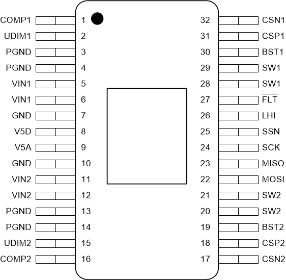
 Figure 5-1 DAD Package32-Pin HTSSOP (Top-Exposed PAD)Top View
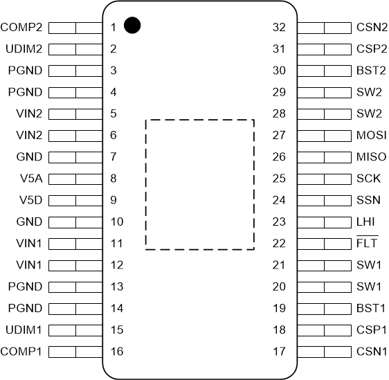
 Figure 5-2 DAP Package 32-Pin HTSSOP
(Top-Exposed PAD) Top View
Figure 5-2 DAP Package 32-Pin HTSSOP
(Top-Exposed PAD) Top ViewTable 5-1 Pin Functions
| PIN | I/O | DESCRIPTION | ||
|---|---|---|---|---|
| NAME | NO. | |||
| DAD | DAP | |||
| BST1 | 30 | 19 | P | Supply input for high-side MOSFET gate drive circuit. Connect a ceramic capacitor between BSTx and SWx pins. An internal diode is connected between V5D and BSTx. |
| BST2 | 19 | 30 | P | |
| COMP1 | 1 | 16 | I/O | Output of internal transconductance error amplifier. Connect an integral compensation network to ensure stability. |
| COMP2 | 16 | 1 | I/O | |
| CSN1 | 32 | 17 | I | Negative input (–) of internal rail-to-rail transconductance error amplifier. Connect directly to the negative node of the LED current sense resistor, RCS. |
| CSN2 | 17 | 32 | I | |
| CSP1 | 31 | 18 | I | Positive input (+) of internal rail-to-rail transconductance error amplifier. Connect directly to the positive node of the LED current sense resistor, RCS. |
| CSP2 | 18 | 31 | I | |
| FLT | 27 | 22 | O | Open-drain fault indicator. Connect to V5D with a resistor to create an active low fault signal output. |
| GND | 7, 10 | 7, 10 | G | Signal ground. Return for the internal voltage reference and analog circuits. Connect to circuit ground to complete return path. |
| LHI | 26 | 23 | I | Limp-home and standalone mode LED current reference set point. The voltage can be used instead of SPI registers to set LED current. The operation is configured through the LHCFG1 register. Setting voltage below 148 mV disables both channels and setting the voltage above 200 mV enables both channels. |
| MISO | 23 | 26 | O | Open-drain SPI slave data output. Connect a 4.7-kΩ resistor to V5D digital supply voltage. |
| MOSI | 22 | 27 | I | SPI slave data input |
| PGND | 3, 4, 13, 14 | 3, 4, 13, 14 | G | Ground returns for low-side MOSFETs |
| SCK | 24 | 25 | I | SPI clock input |
| SSN | 25 | 24 | I | SPI chip select input |
| SW1 | 28, 29 | 20, 21 | P | Switching output of the regulator. Internally connected to both power MOSFETs. Connect to the power inductor. |
| SW2 | 20, 21 | 28, 29 | P | |
| UDIM1 | 2 | 15 | I | Undervoltage lockout and external PWM dimming input. Connect to VIN through a resistor divider to implement input undervoltage protection. Diode couple external PWM signal to enable dimming. Do not float. |
| UDIM2 | 15 | 2 | I | |
| V5A | 9 | 8 | P | Analog supply voltage. Locally decouple to GND using a 100-nF to 1-µF ceramic capacitor located close to the controller. |
| V5D | 8 | 9 | P | Digital supply voltage. Locally decouple to GND using a 2.2-µF to 4.7-µF ceramic capacitor located close to the controller. |
| VIN1 | 5, 6 | 11, 12 | P | Power inputs and connections to high-side MOSFET drain node. Connect to the power supply and bypass capacitors CIN. The path from the VIN pin to high frequency bypass CIN and PGND must be as short as possible. |
| VIN2 | 11, 12 | 5, 6 | P | |