SLUSD66D September 2019 – February 2021 TPS92520-Q1
PRODUCTION DATA
- 1 Features
- 2 Applications
- 3 Description
- 4 Revision History
- 5 Pin Configuration and Functions
- 6 Specifications
-
7 Detailed Description
- 7.1 Overview
- 7.2 Functional Block Diagram
- 7.3
Feature Description
- 7.3.1 Buck Converter Switching Operation
- 7.3.2 Switching Frequency and Adaptive On-Time Control
- 7.3.3 Minimum On-Time, Off-Time, and Inductor Ripple
- 7.3.4 LED Current Regulation and Error Amplifier
- 7.3.5 Start-up Sequence
- 7.3.6 Analog Dimming and Forced Continuous Conduction Mode
- 7.3.7 External PWM Dimming and Input Undervoltage Lockout (UVLO)
- 7.3.8 Internal PWM Dimming
- 7.3.9 Shunt FET Dimming or Matrix Beam Application
- 7.3.10 Bias Supply
- 7.3.11 Bootstrap Supply
- 7.3.12 ADC
- 7.3.13 Faults and Diagnostics
- 7.3.14 Output Short Circuit Fault
- 7.3.15 Output Open Circuit Fault
- 7.4 Device Functional Modes
- 7.5 Programming
- 7.6
Register Maps
- 7.6.1 Configuration Registers
- 7.6.2 STATUS Registers
- 7.6.3
Device Control Registers
- 7.6.3.1 Thermal Warning Limit (address = 0x06) [reset = 0x8A]
- 7.6.3.2 SLEEP Command (address = 0x07) [reset = 0x00]
- 7.6.3.3 CH1IADJL Control Register (address = 0x08) [reset = 0x00]
- 7.6.3.4 CH1IADJH Control Register (address = 0x09) [reset = 0x00]
- 7.6.3.5 CH2IADJL Control Register (address = 0x0A) [reset = 0x00]
- 7.6.3.6 CH2IADJH Control Register (address = 0x0B) [reset = 0x00]
- 7.6.3.7 PWMDIV Register (address = 0x0C) [reset = 0x04]
- 7.6.3.8 CH1PWML Register (address = 0x0D) [reset = 0x00]
- 7.6.3.9 CH1PWMH Register (address = 0x0E) [reset = 0x00]
- 7.6.3.10 CH2PWML Register (address = 0x0F) [reset = 0x00]
- 7.6.3.11 CH2PWMH Register (address = 0x10) [reset = 0x00]
- 7.6.3.12 CH1TON Register (address = 0x11) [reset = 0x07]
- 7.6.3.13 CH2TON Register (address = 0x12) [reset = 0x07]
- 7.6.4
ADC Measurements
- 7.6.4.1 CH1VIN Measurement (address = 0x13)
- 7.6.4.2 CH1VLED Measurement (address = 0x14)
- 7.6.4.3 CH1VLEDON Measurement (address = 0x15)
- 7.6.4.4 CH1VLEDOFF Measurement (address = 0x16)
- 7.6.4.5 CH2VIN Measurement (address = 0x17)
- 7.6.4.6 CH2VLED Measurement (address = 0x18)
- 7.6.4.7 CH2VLEDON Measurement (address = 0x19)
- 7.6.4.8 CH2VLEDOFF Measurement (address = 0x1A)
- 7.6.4.9 TEMPL Measurement (address = 0x1B)
- 7.6.4.10 TEMPH Measurement (address = 0x1C)
- 7.6.4.11 V5D Measurement (address = 0x1D)
- 7.6.5
Limp-Home Configuration and Command Registers
- 7.6.5.1 LHCFG1 Register (address = 0x1E) [reset =0x00]
- 7.6.5.2 LHCFG2 Register (address = 0x1F) [reset =0x00h]
- 7.6.5.3 LHIL Measurement (address = 0x20)
- 7.6.5.4 LHIH Measurement (address = 0x21)
- 7.6.5.5 LHIFILTL Register (address = 0x22)
- 7.6.5.6 LHIFILTH Register (address = 0x23)
- 7.6.5.7 LH1IADJL Register (address = 0x24) [reset = 0x00]
- 7.6.5.8 LH1IADJH Register (address = 0x25) [reset = 0x00]
- 7.6.5.9 LH2IADJL Register (address = 0x26) [reset = 0x00]
- 7.6.5.10 LH2IADJH Register (address = 0x27) [reset = 0x00]
- 7.6.5.11 LH1PWML Register (address = 0x28) [reset = 0x00]
- 7.6.5.12 LH1PWMH Register (address = 0x29) [reset = 0x00]
- 7.6.5.13 LH2PWML Register (address = 0x2A) [reset = 0x00]
- 7.6.5.14 LH2PWMH Register (address = 0x2B) [reset = 0x00]
- 7.6.5.15 LH1TON Register (address = 0x2C) [reset = 0x07]
- 7.6.5.16 LH2TON Register (address = 0x2D) [reset = 0x07]
- 7.6.6 RESET Register (address = 0x2E) (Write-Only)
-
8 Application and Implementation
- 8.1
Application Information
- 8.1.1 Duty Cycle Consideration
- 8.1.2 Switching Frequency Selection
- 8.1.3 LED Current Set Point
- 8.1.4 Inductor Selection
- 8.1.5 Output Capacitor Selection
- 8.1.6 Input Capacitor Selection
- 8.1.7 Bootstrap Capacitor Selection
- 8.1.8 Compensation Capacitor Selection
- 8.1.9 Input Undervoltage Protection
- 8.1.10 CSN Protection Diode
- 8.2
Typical Application
- 8.2.1
Design Requirements
- 8.2.1.1
Detailed Design Procedure
- 8.2.1.1.1 Calculating Duty Cycle
- 8.2.1.1.2 Calculating Minimum On-Time and Off-Time
- 8.2.1.1.3 Minimum Switching Frequency
- 8.2.1.1.4 LED Current Set Point
- 8.2.1.1.5 Inductor Selection
- 8.2.1.1.6 Output Capacitor Selection
- 8.2.1.1.7 Bootstrap Capacitor Selection
- 8.2.1.1.8 Compensation Capacitor Selection
- 8.2.1.1.9 External Channel Enable and PWM dimming
- 8.2.1.1
Detailed Design Procedure
- 8.2.2 Application Curves
- 8.2.1
Design Requirements
- 8.3 Initialization Setup
- 8.1
Application Information
- 9 Power Supply Recommendations
- 10Layout
- 11Device and Documentation Support
- 12Mechanical, Packaging, and Orderable Information
Package Options
Mechanical Data (Package|Pins)
Thermal pad, mechanical data (Package|Pins)
Orderable Information
7.3.7 External PWM Dimming and Input Undervoltage Lockout (UVLO)
The UDIM pin is a dual-function input that features an accurate 1.22-V threshold with programmable hysteresis as shown in Figure 7-4. This pin functions as both the external PWM dimming input for the LEDs and as a VIN UVLO. When the rising pin voltage exceeds the 1.22-V threshold, 10 µA (typical) of current is driven out of the UDIM pin into the resistor divider providing programmable hysteresis.
 Figure 7-4 External PWM Dimming
The brightness of LEDs can be varied by modulating the duty cycle of the signal directly connected to the UDIM input. In addition, either an n-channel MOSFET or a Schottky diode can be used to couple an external PWM signal when using UDIM input in conjunction with UVLO functionality. With an n-channel MOSFET, the brightness is proportional to the negative duty cycle of the external PWM signal. With an Schottky diode, the brightness is proportional to the positive duty cycle of the external PWM signal.
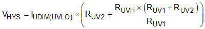
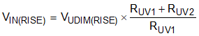
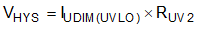
When using the UDIM pin for UVLO and PWM dimming concurrently, the UVLO circuit can have an extra resistor to set the hysteresis. This allows the standard resistor divider to have smaller values, minimizing PWM delays. TI recommends at least 1 V of hysteresis when PWM dimming if you are operating near the UVLO threshold. Use Equation 8 to define the rising threshold.
Use Equation 9 to define the hysteresis.
UVLO only:
PWM and UVLO: