SLUSD66D September 2019 – February 2021 TPS92520-Q1
PRODUCTION DATA
- 1 Features
- 2 Applications
- 3 Description
- 4 Revision History
- 5 Pin Configuration and Functions
- 6 Specifications
-
7 Detailed Description
- 7.1 Overview
- 7.2 Functional Block Diagram
- 7.3
Feature Description
- 7.3.1 Buck Converter Switching Operation
- 7.3.2 Switching Frequency and Adaptive On-Time Control
- 7.3.3 Minimum On-Time, Off-Time, and Inductor Ripple
- 7.3.4 LED Current Regulation and Error Amplifier
- 7.3.5 Start-up Sequence
- 7.3.6 Analog Dimming and Forced Continuous Conduction Mode
- 7.3.7 External PWM Dimming and Input Undervoltage Lockout (UVLO)
- 7.3.8 Internal PWM Dimming
- 7.3.9 Shunt FET Dimming or Matrix Beam Application
- 7.3.10 Bias Supply
- 7.3.11 Bootstrap Supply
- 7.3.12 ADC
- 7.3.13 Faults and Diagnostics
- 7.3.14 Output Short Circuit Fault
- 7.3.15 Output Open Circuit Fault
- 7.4 Device Functional Modes
- 7.5 Programming
- 7.6
Register Maps
- 7.6.1 Configuration Registers
- 7.6.2 STATUS Registers
- 7.6.3
Device Control Registers
- 7.6.3.1 Thermal Warning Limit (address = 0x06) [reset = 0x8A]
- 7.6.3.2 SLEEP Command (address = 0x07) [reset = 0x00]
- 7.6.3.3 CH1IADJL Control Register (address = 0x08) [reset = 0x00]
- 7.6.3.4 CH1IADJH Control Register (address = 0x09) [reset = 0x00]
- 7.6.3.5 CH2IADJL Control Register (address = 0x0A) [reset = 0x00]
- 7.6.3.6 CH2IADJH Control Register (address = 0x0B) [reset = 0x00]
- 7.6.3.7 PWMDIV Register (address = 0x0C) [reset = 0x04]
- 7.6.3.8 CH1PWML Register (address = 0x0D) [reset = 0x00]
- 7.6.3.9 CH1PWMH Register (address = 0x0E) [reset = 0x00]
- 7.6.3.10 CH2PWML Register (address = 0x0F) [reset = 0x00]
- 7.6.3.11 CH2PWMH Register (address = 0x10) [reset = 0x00]
- 7.6.3.12 CH1TON Register (address = 0x11) [reset = 0x07]
- 7.6.3.13 CH2TON Register (address = 0x12) [reset = 0x07]
- 7.6.4
ADC Measurements
- 7.6.4.1 CH1VIN Measurement (address = 0x13)
- 7.6.4.2 CH1VLED Measurement (address = 0x14)
- 7.6.4.3 CH1VLEDON Measurement (address = 0x15)
- 7.6.4.4 CH1VLEDOFF Measurement (address = 0x16)
- 7.6.4.5 CH2VIN Measurement (address = 0x17)
- 7.6.4.6 CH2VLED Measurement (address = 0x18)
- 7.6.4.7 CH2VLEDON Measurement (address = 0x19)
- 7.6.4.8 CH2VLEDOFF Measurement (address = 0x1A)
- 7.6.4.9 TEMPL Measurement (address = 0x1B)
- 7.6.4.10 TEMPH Measurement (address = 0x1C)
- 7.6.4.11 V5D Measurement (address = 0x1D)
- 7.6.5
Limp-Home Configuration and Command Registers
- 7.6.5.1 LHCFG1 Register (address = 0x1E) [reset =0x00]
- 7.6.5.2 LHCFG2 Register (address = 0x1F) [reset =0x00h]
- 7.6.5.3 LHIL Measurement (address = 0x20)
- 7.6.5.4 LHIH Measurement (address = 0x21)
- 7.6.5.5 LHIFILTL Register (address = 0x22)
- 7.6.5.6 LHIFILTH Register (address = 0x23)
- 7.6.5.7 LH1IADJL Register (address = 0x24) [reset = 0x00]
- 7.6.5.8 LH1IADJH Register (address = 0x25) [reset = 0x00]
- 7.6.5.9 LH2IADJL Register (address = 0x26) [reset = 0x00]
- 7.6.5.10 LH2IADJH Register (address = 0x27) [reset = 0x00]
- 7.6.5.11 LH1PWML Register (address = 0x28) [reset = 0x00]
- 7.6.5.12 LH1PWMH Register (address = 0x29) [reset = 0x00]
- 7.6.5.13 LH2PWML Register (address = 0x2A) [reset = 0x00]
- 7.6.5.14 LH2PWMH Register (address = 0x2B) [reset = 0x00]
- 7.6.5.15 LH1TON Register (address = 0x2C) [reset = 0x07]
- 7.6.5.16 LH2TON Register (address = 0x2D) [reset = 0x07]
- 7.6.6 RESET Register (address = 0x2E) (Write-Only)
-
8 Application and Implementation
- 8.1
Application Information
- 8.1.1 Duty Cycle Consideration
- 8.1.2 Switching Frequency Selection
- 8.1.3 LED Current Set Point
- 8.1.4 Inductor Selection
- 8.1.5 Output Capacitor Selection
- 8.1.6 Input Capacitor Selection
- 8.1.7 Bootstrap Capacitor Selection
- 8.1.8 Compensation Capacitor Selection
- 8.1.9 Input Undervoltage Protection
- 8.1.10 CSN Protection Diode
- 8.2
Typical Application
- 8.2.1
Design Requirements
- 8.2.1.1
Detailed Design Procedure
- 8.2.1.1.1 Calculating Duty Cycle
- 8.2.1.1.2 Calculating Minimum On-Time and Off-Time
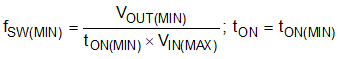
- 8.2.1.1.3 Minimum Switching Frequency
- 8.2.1.1.4 LED Current Set Point
- 8.2.1.1.5 Inductor Selection
- 8.2.1.1.6 Output Capacitor Selection
- 8.2.1.1.7 Bootstrap Capacitor Selection
- 8.2.1.1.8 Compensation Capacitor Selection
- 8.2.1.1.9 External Channel Enable and PWM dimming
- 8.2.1.1
Detailed Design Procedure
- 8.2.2 Application Curves
- 8.2.1
Design Requirements
- 8.3 Initialization Setup
- 8.1
Application Information
- 9 Power Supply Recommendations
- 10Layout
- 11Device and Documentation Support
- 12Mechanical, Packaging, and Orderable Information
Package Options
Mechanical Data (Package|Pins)
Thermal pad, mechanical data (Package|Pins)
Orderable Information
7.3.3 Minimum On-Time, Off-Time, and Inductor Ripple
Buck converter operation is impacted by minimum on-time, minimum off-time, and minimum peak-to-peak inductor ripple limitations. The converter reaches the minimum on-time of 105 ns (typ) when operating with high input voltage and low-output voltage. In this control scheme, the off-time continues to increase and the switching frequency reduces to regulate the inductor current and LED current to the desired value.
The converter reaches the minimum off-time of 57 ns (typ) when operating in dropout (low input voltage and high output voltage). As the on-time and off-time are fixed, the duty cycle is constant and the buck converter operates in open-loop mode. The inductor current and LED current are not in regulation. The CHxTOFFMIN bit is set to indicate operation at maximum duty cycle. The converter continues to switch unless disabled by resetting the CHxEN bit. Upon detection of a minimum off-time operation, the device disables the error amplifier and disconnects the COMP pin to maintain charge on the compensation network. This ensures fast response with minimum LED current overshoot as the converter recovers from dropout condition.
The behavior and response of valley comparator is dependent on sensed peak-to-peak voltage ripple, ΔV(CSP-CSN), and is a function of current sense resistor, RCS, and peak-to-peak inductor current ripple, ΔiL(PK-PK). To ensure periodic switching, the sensed peak-to-peak ripple needs to exceed the minimum value, specified in Figure 6-5. At high (near 100%) or low (near 0%) duty cycles, the inductor current ripple may not be sufficient to ensure periodic switching. Under such operating conditions, the converter transitions from periodic switching to a burst sequence, forcing multiple on-time and off-time cycles at a rate higher than the programmed frequency. Although the converter may not operate in a periodic manner, the closed-loop control continues regulating the average LED current with a larger ripple value corresponding to higher peak-to-peak inductor ripple. TI recommends choosing an inductor, output capacitor, and switching frequency to ensure minimum sensed peak-to-peak ripple voltage under nominal operating condition is greater than 20 mV. The Application and Implementation section summarizes the detailed design procedure.