SLUSD66D September 2019 – February 2021 TPS92520-Q1
PRODUCTION DATA
- 1 Features
- 2 Applications
- 3 Description
- 4 Revision History
- 5 Pin Configuration and Functions
- 6 Specifications
-
7 Detailed Description
- 7.1 Overview
- 7.2 Functional Block Diagram
- 7.3
Feature Description
- 7.3.1 Buck Converter Switching Operation
- 7.3.2 Switching Frequency and Adaptive On-Time Control
- 7.3.3 Minimum On-Time, Off-Time, and Inductor Ripple
- 7.3.4 LED Current Regulation and Error Amplifier
- 7.3.5 Start-up Sequence
- 7.3.6 Analog Dimming and Forced Continuous Conduction Mode
- 7.3.7 External PWM Dimming and Input Undervoltage Lockout (UVLO)
- 7.3.8 Internal PWM Dimming
- 7.3.9 Shunt FET Dimming or Matrix Beam Application
- 7.3.10 Bias Supply
- 7.3.11 Bootstrap Supply
- 7.3.12 ADC
- 7.3.13 Faults and Diagnostics
- 7.3.14 Output Short Circuit Fault
- 7.3.15 Output Open Circuit Fault
- 7.4 Device Functional Modes
- 7.5 Programming
- 7.6
Register Maps
- 7.6.1 Configuration Registers
- 7.6.2 STATUS Registers
- 7.6.3
Device Control Registers
- 7.6.3.1 Thermal Warning Limit (address = 0x06) [reset = 0x8A]
- 7.6.3.2 SLEEP Command (address = 0x07) [reset = 0x00]
- 7.6.3.3 CH1IADJL Control Register (address = 0x08) [reset = 0x00]
- 7.6.3.4 CH1IADJH Control Register (address = 0x09) [reset = 0x00]
- 7.6.3.5 CH2IADJL Control Register (address = 0x0A) [reset = 0x00]
- 7.6.3.6 CH2IADJH Control Register (address = 0x0B) [reset = 0x00]
- 7.6.3.7 PWMDIV Register (address = 0x0C) [reset = 0x04]
- 7.6.3.8 CH1PWML Register (address = 0x0D) [reset = 0x00]
- 7.6.3.9 CH1PWMH Register (address = 0x0E) [reset = 0x00]
- 7.6.3.10 CH2PWML Register (address = 0x0F) [reset = 0x00]
- 7.6.3.11 CH2PWMH Register (address = 0x10) [reset = 0x00]
- 7.6.3.12 CH1TON Register (address = 0x11) [reset = 0x07]
- 7.6.3.13 CH2TON Register (address = 0x12) [reset = 0x07]
- 7.6.4
ADC Measurements
- 7.6.4.1 CH1VIN Measurement (address = 0x13)
- 7.6.4.2 CH1VLED Measurement (address = 0x14)
- 7.6.4.3 CH1VLEDON Measurement (address = 0x15)
- 7.6.4.4 CH1VLEDOFF Measurement (address = 0x16)
- 7.6.4.5 CH2VIN Measurement (address = 0x17)
- 7.6.4.6 CH2VLED Measurement (address = 0x18)
- 7.6.4.7 CH2VLEDON Measurement (address = 0x19)
- 7.6.4.8 CH2VLEDOFF Measurement (address = 0x1A)
- 7.6.4.9 TEMPL Measurement (address = 0x1B)
- 7.6.4.10 TEMPH Measurement (address = 0x1C)
- 7.6.4.11 V5D Measurement (address = 0x1D)
- 7.6.5
Limp-Home Configuration and Command Registers
- 7.6.5.1 LHCFG1 Register (address = 0x1E) [reset =0x00]
- 7.6.5.2 LHCFG2 Register (address = 0x1F) [reset =0x00h]
- 7.6.5.3 LHIL Measurement (address = 0x20)
- 7.6.5.4 LHIH Measurement (address = 0x21)
- 7.6.5.5 LHIFILTL Register (address = 0x22)
- 7.6.5.6 LHIFILTH Register (address = 0x23)
- 7.6.5.7 LH1IADJL Register (address = 0x24) [reset = 0x00]
- 7.6.5.8 LH1IADJH Register (address = 0x25) [reset = 0x00]
- 7.6.5.9 LH2IADJL Register (address = 0x26) [reset = 0x00]
- 7.6.5.10 LH2IADJH Register (address = 0x27) [reset = 0x00]
- 7.6.5.11 LH1PWML Register (address = 0x28) [reset = 0x00]
- 7.6.5.12 LH1PWMH Register (address = 0x29) [reset = 0x00]
- 7.6.5.13 LH2PWML Register (address = 0x2A) [reset = 0x00]
- 7.6.5.14 LH2PWMH Register (address = 0x2B) [reset = 0x00]
- 7.6.5.15 LH1TON Register (address = 0x2C) [reset = 0x07]
- 7.6.5.16 LH2TON Register (address = 0x2D) [reset = 0x07]
- 7.6.6 RESET Register (address = 0x2E) (Write-Only)
-
8 Application and Implementation
- 8.1
Application Information
- 8.1.1 Duty Cycle Consideration
- 8.1.2 Switching Frequency Selection
- 8.1.3 LED Current Set Point
- 8.1.4 Inductor Selection
- 8.1.5 Output Capacitor Selection
- 8.1.6 Input Capacitor Selection
- 8.1.7 Bootstrap Capacitor Selection
- 8.1.8 Compensation Capacitor Selection
- 8.1.9 Input Undervoltage Protection
- 8.1.10 CSN Protection Diode
- 8.2
Typical Application
- 8.2.1
Design Requirements
- 8.2.1.1
Detailed Design Procedure
- 8.2.1.1.1 Calculating Duty Cycle
- 8.2.1.1.2 Calculating Minimum On-Time and Off-Time
- 8.2.1.1.3 Minimum Switching Frequency
- 8.2.1.1.4 LED Current Set Point
- 8.2.1.1.5 Inductor Selection
- 8.2.1.1.6 Output Capacitor Selection
- 8.2.1.1.7 Bootstrap Capacitor Selection
- 8.2.1.1.8 Compensation Capacitor Selection
- 8.2.1.1.9 External Channel Enable and PWM dimming
- 8.2.1.1
Detailed Design Procedure
- 8.2.2 Application Curves
- 8.2.1
Design Requirements
- 8.3 Initialization Setup
- 8.1
Application Information
- 9 Power Supply Recommendations
- 10Layout
- 11Device and Documentation Support
- 12Mechanical, Packaging, and Orderable Information
Package Options
Mechanical Data (Package|Pins)
Thermal pad, mechanical data (Package|Pins)
Orderable Information
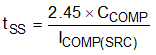
7.3.5 Start-up Sequence
The start-up circuit allows the COMP pin voltage to gradually increase, thus reducing the LED current overshoot and current surges. The switching operation is initiated after the COMP pin voltage exceeds 2.45 V. A 250-mV hysteresis window allows the device to operate when COMP voltage is within the expected operating range of 2.2 V to 2.7 V. Switching is disabled on detection of low COMP voltage to avoid excessive negative inductor current.
 Figure 7-3 Soft-Start Sequence
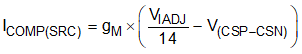
The duration of soft start, tss, depends on the size of the compensation capacitor and the error amplifier source current, ICOMP(SRC).
The source current, ICOMP(SRC) is a function of the transconductance, gM, of the error amplifier and error generated between the reference and the current sensed voltage.
With no current flowing through the LEDs, the soft start duration depends on the choice of compensation capacitor, CCOMP, and the reference voltage, VIADJ.
The CHxCOMPOV bit in the STATUS1 register is set when the COMP voltage deviates from the nominal range and exceeds 3.2 V. This indicates a fault condition where the converter is operating in open-loop and the LED current is out of regulation. The corresponding channel can be disabled by resetting the CHxEN bit via a SPI command or controlling the UDIMx input.