at TA = 25℃, VS+
= 5V, VS– = 0V, floating VOCM, PD, and MODE pins, VICM =
mid-supply, D2D ac-coupled input/output configuration with ZS = 100Ω,
ZL = 100Ω, external input resistor network (see Figure 8-6), inputs de-embedded up to RIN_SH and outputs up to the device pins,
ambient temperatures shown, and resistor network included as part of DUT
characteristic plots (unless otherwise noted)

| PIN = –20dBm with 50Ω source at all
excited ports, |
| nonexcited ports are terminated with 50Ω |
Figure 6-1 Power
Gain (Sdd21) Across Temperature 
| PIN = –20dBm with 50Ω source at all
excited ports, |
| nonexcited ports are terminated with 50Ω |
Figure 6-3 Input
Return Loss (Sdd11) Across Temperature
| PIN = –20dBm with 50Ω source at all
excited ports, |
| nonexcited ports are terminated with 50Ω |
Figure 6-5 Output Return Loss (Sdd22) Across Temperature
| PIN = –20dBm with 50Ω source at all
excited ports, |
| nonexcited ports are terminated with 50Ω |
Figure 6-7 Reverse Isolation (Sdd12) Across Temperature
| PO = –5dBm/tone, 2MHz tone
spacing |
Figure 6-9 OIP3
Across Temperature
|
PO = 1dBm/tone,
2MHz tone spacing |
|
Figure 6-11 OIP3
Across Temperature
| At (2f1 –
f2) frequency where f1 <
f2, |
| PO = 1dBm/tone,
2MHz tone spacing |
Figure 6-13 IMD3
Lower Across Temperature
| At (2f2 –
f1) frequency where f1 <
f2, |
| PO = 1dBm/tone,
2MHz tone spacing |
Figure 6-15 IMD3
Higher Across Temperature
| At (2f1 –
f2) frequency where f1 <
f2, |
| PO = –5dBm/tone,
2MHz tone spacing |
Figure 6-17 IMD3
Lower Across Temperature
| At (2f2 –
f1) frequency where f1 <
f2, |
| PO = –5dBm/tone,
2MHz tone spacing |
Figure 6-19 IMD3
Higher Across Temperature
| PO = –5dBm/tone,
2MHz tone spacing |
Figure 6-21 OIP2
Across Temperature
| PO = 1dBm/tone,
2MHz tone spacing |
Figure 6-23 OIP2
Across Temperature
| At (f2 –
f1) frequency where f1 <
f2, |
| PO = 1dBm/tone,
2MHz tone spacing |
Figure 6-25 IMD2
Lower Across Temperature
| At (f1 +
f2) frequency where f1 <
f2, |
| PO = 1dBm/tone,
2MHz tone spacing |
Figure 6-27 IMD2
Higher Across Temperature
| At (f2 –
f1) frequency where f1 <
f2, |
| PO = –5dBm/tone,
2MHz tone spacing |
Figure 6-29 IMD2
Lower Across Temperature
| At (f1 +
f2) frequency where f1 <
f2, |
| PO = –5dBm/tone,
2MHz tone spacing |
Figure 6-31 IMD2
Higher Across Temperature Figure 6-33 HD2
Across Temperature
 Figure 6-35 HD2
Across Temperature
 Figure 6-37 HD3
Across Temperature
 Figure 6-39 HD3
Across Temperature
 Figure 6-41 OP1dB
Across Temperature
 Figure 6-43 Noise
Figure Across Temperature
| PO = 1dBm/tone,
2MHz tone spacing, dc-coupled inputs with
VICM forced through bias tees |
Figure 6-45 OIP3
Across VICM and VOCM at 500MHz, Ch1
| PO = 1dBm/tone,
2MHz tone spacing, dc-coupled inputs with
VICM forced through bias tees |
Figure 6-47 OIP3
Across VICM and VOCM at 2GHz, Ch1
| PO = 1dBm/tone,
2MHz tone spacing, dc-coupled inputs with
VICM forced through bias tees |
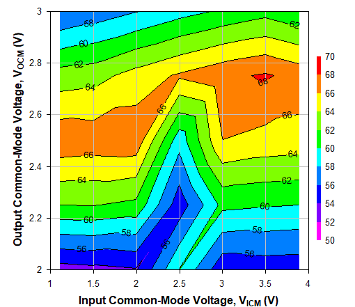
Figure 6-49 OIP2
Across VICM and VOCM at 500MHz, Ch1
| PO = 1dBm/tone,
2MHz tone spacing, dc-coupled inputs with
VICM forced through bias tees |
Figure 6-51 OIP2
Across VICM and VOCM at 2GHz, Ch1
| dc-coupled inputs with
VICM forced through bias tees |
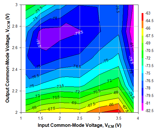
Figure 6-53 OP1dB
Across VICM and VOCM at 500MHz, Ch1
| dc-coupled inputs with
VICM forced through bias tees |
Figure 6-55 OP1dB
Across VICM and VOCM at 2GHz, Ch1
| PO = 7dBm,
dc-coupled inputs with |
| VICM forced
through bias tees |
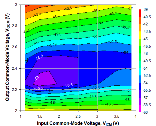
Figure 6-57 HD2
Across VICM and VOCM at 500MHz, Ch1
| PO = 7dBm,
dc-coupled inputs with |
| VICM forced
through bias tees |
Figure 6-59 HD2
Across VICM and VOCM at 2GHz, Ch1
| PO = 7dBm,
dc-coupled inputs with |
| VICM forced
through bias tees |
Figure 6-61 HD3
Across VICM and VOCM at 500MHz, Ch1
| PO = 7dBm,
dc-coupled inputs with |
| VICM forced
through bias tees |
Figure 6-63 HD3
Across VICM and VOCM at 2GHz, Ch1
| DC-coupled, VS+
= 2.5V, VS– = –2.5V |
Figure 6-65 Step
Response Figure 6-67 Differential Output Power Across Differential Input Power, Ch1
| PIN = –20dBm at
each driven input pin with 50Ω source, c in Sdc21
and Scc21 is for common-mode |
Figure 6-69 Common-Mode Rejection Ratio (CMRR) 
| DC-coupled,
VS+ = 2.5V, VS– = –2.5V, 2 to
5 times output voltages are with an input voltage 2 to 5
times of VIN as shown, respectively |
Figure 6-71 Overdrive Recovery Response, Ch1
| PIN =
–20dBm at each driven input pin with 50Ω source |
Figure 6-73 Crosstalk
| PIN = –20dBm with 50Ω source at all
excited ports, |
| nonexcited ports are terminated with 50Ω |
Figure 6-2 Power
Gain (Sdd21) Across Supply Voltage
| PIN = –20dBm with 50Ω source at all
excited ports, |
| nonexcited ports are terminated with 50Ω |
Figure 6-4 Input
Return Loss (Sdd11) Across Supply Voltage
| PIN = –20dBm with 50Ω source at all
excited ports, |
| nonexcited ports are terminated with 50Ω |
Figure 6-6 Output Return Loss (Sdd22) Across Supply Voltage
| PIN = –20dBm with 50Ω source at all
excited ports, |
| nonexcited ports are terminated with 50Ω |
Figure 6-8 Reverse Isolation (Sdd12) Across Supply Voltage
| PO = –5dBm/tone, 2MHz tone
spacing |
Figure 6-10 OIP3
Across Supply Voltage
|
PO = 1dBm/tone,
2MHz tone spacing |
|
Figure 6-12 OIP3
Across Supply Voltage
| At (2f1 –
f2) frequency where f1 <
f2, |
| PO = 1dBm/tone,
2MHz tone spacing |
Figure 6-14 IMD3
Lower Across Supply Voltage
| At (2f2 –
f1) frequency where f1 <
f2, |
| PO = 1dBm/tone,
2MHz tone spacing |
Figure 6-16 IMD3
Higher Across Supply Voltage
| At (2f1 –
f2) frequency where f1 <
f2, |
| PO = –5dBm/tone,
2MHz tone spacing |
Figure 6-18 IMD3
Lower Across Supply Voltage
| At (2f2 –
f1) frequency where f1 <
f2, |
| PO = –5dBm/tone,
2MHz tone spacing |
Figure 6-20 IMD3
Higher Across Supply Voltage
| PO = –5dBm/tone,
2MHz tone spacing |
Figure 6-22 OIP2
Across Supply Voltage
| PO = 1dBm/tone,
2MHz tone spacing |
Figure 6-24 OIP2
Across Supply Voltage
| At (f2 –
f1) frequency where f1 <
f2, |
| PO = 1dBm/tone,
2MHz tone spacing |
Figure 6-26 IMD2
Lower Across Supply Voltage
| At (f1 +
f2) frequency where f1 <
f2, |
| PO = 1dBm/tone,
2MHz tone spacing |
Figure 6-28 IMD2
Higher Across Supply Voltage
| At (f2 –
f1) frequency where f1 <
f2, |
| PO = –5dBm/tone,
2MHz tone spacing |
Figure 6-30 IMD2
Lower Across Supply Voltage
| At (f1 +
f2) frequency where f1 <
f2, |
| PO = –5dBm/tone,
2MHz tone spacing |
Figure 6-32 IMD2
Higher Across Supply Voltage Figure 6-34 HD2
Across Supply Voltage
 Figure 6-36 HD2
Across Supply Voltage
 Figure 6-38 HD3
Across Supply Voltage
 Figure 6-40 HD3
Across Supply Voltage
 Figure 6-42 OP1dB
Across Supply Voltage
 Figure 6-44 Noise
Figure Across Supply Voltage
| PO = 1dBm/tone,
2MHz tone spacing, dc-coupled inputs with
VICM forced through bias tees |
Figure 6-46 OIP3
Across VICM and VOCM at 500MHz, Ch2
| PO = 1dBm/tone,
2MHz tone spacing, dc-coupled inputs with
VICM forced through bias tees |
Figure 6-48 OIP3
Across VICM and VOCM at 2GHz, Ch2
| PO = 1dBm/tone,
2MHz tone spacing, dc-coupled inputs with
VICM forced through bias tees |
Figure 6-50 OIP2
Across VICM and VOCM at 500MHz, Ch2
| PO = 1dBm/tone,
2MHz tone spacing, dc-coupled inputs with
VICM forced through bias tees |
Figure 6-52 OIP2
Across VICM and VOCM at 2GHz, Ch2
| dc-coupled inputs with
VICM forced through bias tees |
Figure 6-54 OP1dB
Across VICM and VOCM at 500MHz, Ch2
| dc-coupled inputs with
VICM forced through bias tees |
Figure 6-56 OP1dB
Across VICM and VOCM at 2GHz, Ch2
| PO = 7dBm,
dc-coupled inputs with |
| VICM forced
through bias tees |
Figure 6-58 HD2
Across VICM and VOCM at 500MHz, Ch2
| PO = 7dBm,
dc-coupled inputs with |
| VICM forced
through bias tees |
Figure 6-60 HD2
Across VICM and VOCM at 2GHz, Ch2
| PO = 7dBm,
dc-coupled inputs with |
| VICM forced
through bias tees |
Figure 6-62 HD3
Across VICM and VOCM at 500MHz, Ch2
| PO = 7dBm,
dc-coupled inputs with |
| VICM forced
through bias tees |
Figure 6-64 HD3
Across VICM and VOCM at 2GHz, Ch2
| DC-coupled, VS+
= 2.5V, VS– = –2.5V |
Figure 6-66 Step
Response Figure 6-68 Differential Output Power Across Differential Input Power, Ch2
| PIN =
–20dBm at each driven input pin with 50Ω source |
| |
Figure 6-70 Gain
and Phase Mismatch Between Channels
| DC-coupled,
VS+ = 2.5V, VS– = –2.5V, 2 to
5 times output voltages are with an input voltage 2 to 5
times of VIN as shown, respectively |
Figure 6-72 Overdrive Recovery Response, Ch2


