SLOSEG3 October 2025 TRF1305A2
PRODUCTION DATA
- 1
- 1 Features
- 2 Applications
- 3 Description
- 4 Device Comparison Table
- 5 Pin Configuration and Functions
-
6 Specifications
- 6.1 Absolute Maximum Ratings
- 6.2 ESD Ratings
- 6.3 Recommended Operating Conditions
- 6.4 Thermal Information
- 6.5 Electrical Characteristics - AC Specifications in D2D Configuration
- 6.6 Electrical Characteristics - AC Specifications in S2D Configuration
- 6.7 Electrical Characteristics - DC and Timing Specifications
- 6.8 Typical Characteristics: D2D Configuration
- 6.9 Typical Characteristics: S2D Configuration
- 7 Detailed Description
- 8 Application and Implementation
- 9 Device and Documentation Support
- 10Revision History
- 11Mechanical, Packaging, and Orderable Information
Package Options
Refer to the PDF data sheet for device specific package drawings
Mechanical Data (Package|Pins)
- RYP|16
Thermal pad, mechanical data (Package|Pins)
Orderable Information
3 Description
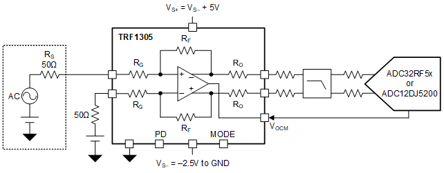
The TRF1305A2 is a very high performance, closed-loop, dual-channel RF amplifier that has an operational bandwidth from true-dc to > 5.8GHz. The device has excellent performance to drive high-speed, high-performance ADCs, such as the ADC12DJ5200RF and ADC32RF5x with a dc- or ac-coupled interface. The amplifier is optimized for use in RF, zero and complex IF, and high-speed time-domain applications. The device is optimized for performance in the fixed gain configuration. If lower gain is desired, use external resistors.
The TRF1305A2 features a VOCM pin that allows setting different output common-mode and input common-mode voltages; for example, level-shifting or for most IQ down-converter ADC-interface applications that have differing dc common-mode voltages. The TRF1305A2 also features a floating two-rail split or single-supply option, and a MODE pin that allows extending the input common-mode range closer to the supplies. The device also has a power-down feature to turn-off each channel individually.
The device uses TI's proprietary advanced BiCMOS process and is available in a space-saving, 2.5mm × 3mm, 16-pin, WQFN-FCRLF package.
| PART NUMBER(1) | POWER GAIN | PACKAGE(2) |
|---|---|---|
| TRF1305A2 | 15dB | RYP (WQFN-FCRLF, 16) |
| TRF1305B2 | 10dB | |
| TRF1305C2 | 5dB |
 TRF1305A2 in S2D Configuration Driving a High-Speed ADC