SLUSA12G December   2009  – November 2022 UCC28C40-Q1 , UCC28C41-Q1 , UCC28C42-Q1 , UCC28C43-Q1 , UCC28C44-Q1 , UCC28C45-Q1

PRODUCTION DATA  

  1. Features
  2. Applications
  3. Description
  4. Revision History
  5. Device Comparison Table
  6. Pin Configuration and Functions
  7. Specifications
    1. 7.1 Absolute Maximum Ratings
    2. 7.2 ESD Ratings
    3. 7.3 Recommended Operating Conditions
    4. 7.4 Thermal Information
    5. 7.5 Electrical Characteristics
    6. 7.6 Typical Characteristics
  8. Detailed Description
    1. 8.1 Overview
    2. 8.2 Functional Block Diagram
    3. 8.3 Feature Description
      1. 8.3.1  Detailed Pin Description
        1. 8.3.1.1 COMP
        2. 8.3.1.2 FB
        3. 8.3.1.3 CS
        4. 8.3.1.4 RT/CT
        5. 8.3.1.5 GND
        6. 8.3.1.6 OUT
        7. 8.3.1.7 VDD
        8. 8.3.1.8 VREF
      2. 8.3.2  Undervoltage Lockout
      3. 8.3.3  ±1% Internal Reference Voltage
      4. 8.3.4  Current Sense and Overcurrent Limit
      5. 8.3.5  Reduced-Discharge Current Variation
      6. 8.3.6  Oscillator Synchronization
      7. 8.3.7  Soft Start
      8. 8.3.8  Enable and Disable
      9. 8.3.9  Slope Compensation
      10. 8.3.10 Voltage Mode
    4. 8.4 Device Functional Modes
      1. 8.4.1 Normal Operation
      2. 8.4.2 UVLO Mode
  9. Application and Implementation
    1. 9.1 Application Information
    2. 9.2 Typical Application
      1. 9.2.1 Design Requirements
      2. 9.2.2 Detailed Design Procedure
        1. 9.2.2.1  Custom Design With WEBENCH® Tools
        2. 9.2.2.2  Input Bulk Capacitor and Minimum Bulk Voltage
        3. 9.2.2.3  Transformer Turns Ratio and Maximum Duty CycleG
        4. 9.2.2.4  Transformer Inductance and Peak Currents
        5. 9.2.2.5  Output Capacitor
        6. 9.2.2.6  Current Sensing Network
        7. 9.2.2.7  Gate Drive Resistor
        8. 9.2.2.8  VREF Capacitor
        9. 9.2.2.9  RT/CT
        10. 9.2.2.10 Start-Up Circuit
        11. 9.2.2.11 Voltage Feedback Compensation
          1. 9.2.2.11.1 Power Stage Poles and Zeroes
          2. 9.2.2.11.2 Slope Compensation
          3. 9.2.2.11.3 Open-Loop Gain
          4. 9.2.2.11.4 Compensation Loop
      3. 9.2.3 Application Curves
      4. 9.2.4 Power Supply Recommendations
      5. 9.2.5 Layout
        1. 9.2.5.1 Layout Guidelines
          1. 9.2.5.1.1 Precautions
          2. 9.2.5.1.2 Feedback Traces
          3. 9.2.5.1.3 Bypass Capacitors
          4. 9.2.5.1.4 Compensation Components
          5. 9.2.5.1.5 Traces and Ground Planes
        2. 9.2.5.2 Layout Example
  10. 10Device and Documentation Support
    1. 10.1 Device Support
      1. 10.1.1 Development Support
        1. 10.1.1.1 Custom Design With WEBENCH® Tools
    2. 10.2 Documentation Support
      1. 10.2.1 Related Documentation
    3. 10.3 Related Links
    4. 10.4 Support Resources
    5. 10.5 Trademarks
    6. 10.6 Electrostatic Discharge Caution
    7. 10.7 Glossary
  11. 11Mechanical, Packaging, and Orderable Information

Package Options

Mechanical Data (Package|Pins)
Thermal pad, mechanical data (Package|Pins)
Orderable Information

Application Curves

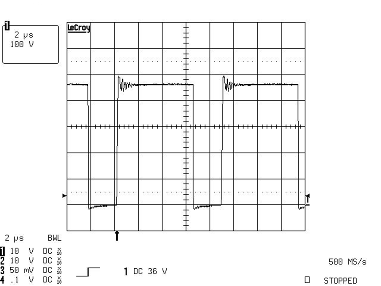
GUID-630B799F-A5E3-4775-B832-7002F00F27AD-low.pngFigure 9-7 Primary Side MOSFET Drain to Source Voltage at 240-V AC Input (100 V/div)
GUID-B8931BA3-C743-4608-98EE-2DEDAF4E601E-low.png
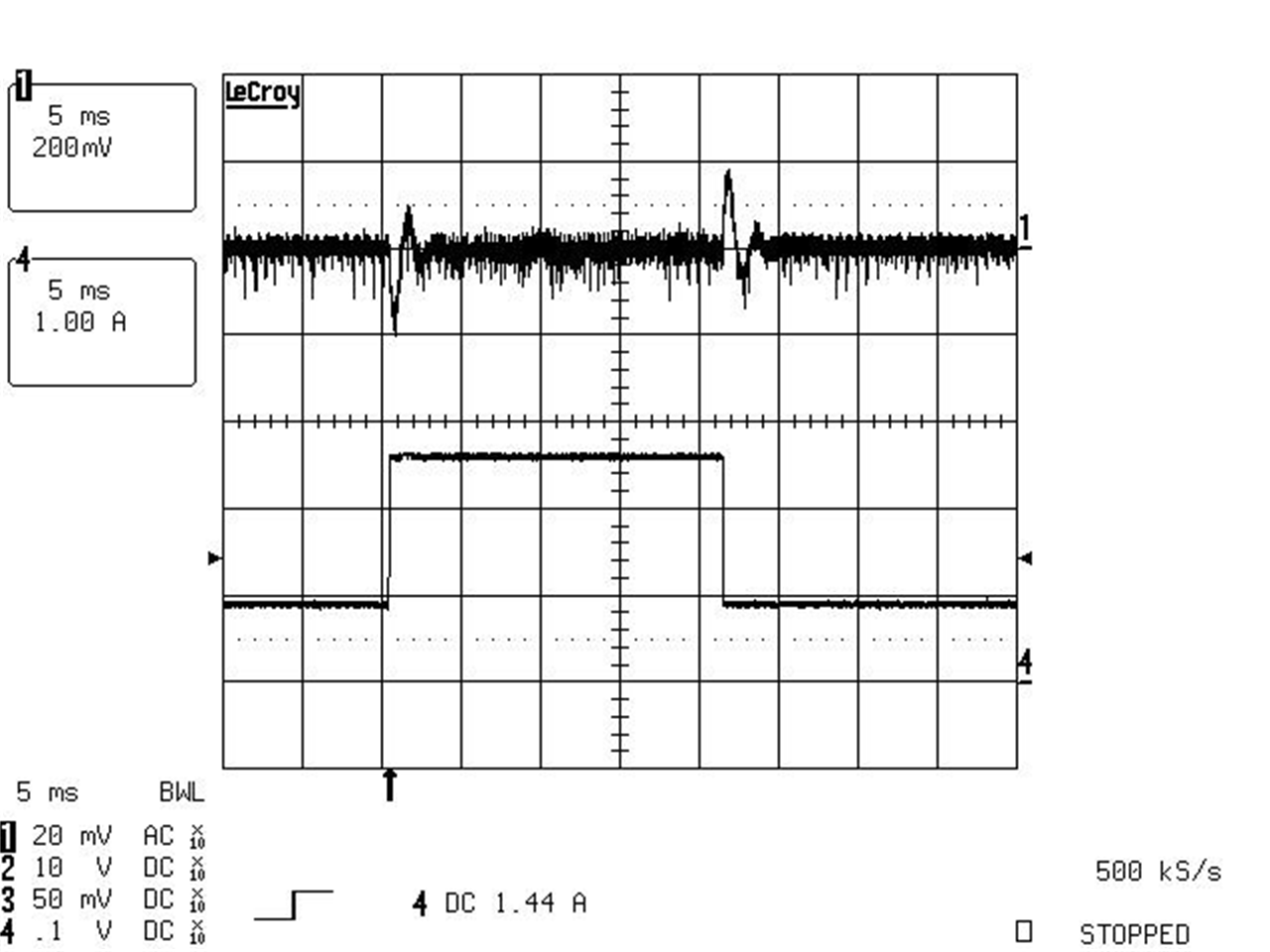
CH1: Output Voltage AC Coupled, 200 mV/div
CH4: Output Current, 1 A/div
Figure 9-9 Output Voltage During 0.9-A to 2.7-A Load Transient
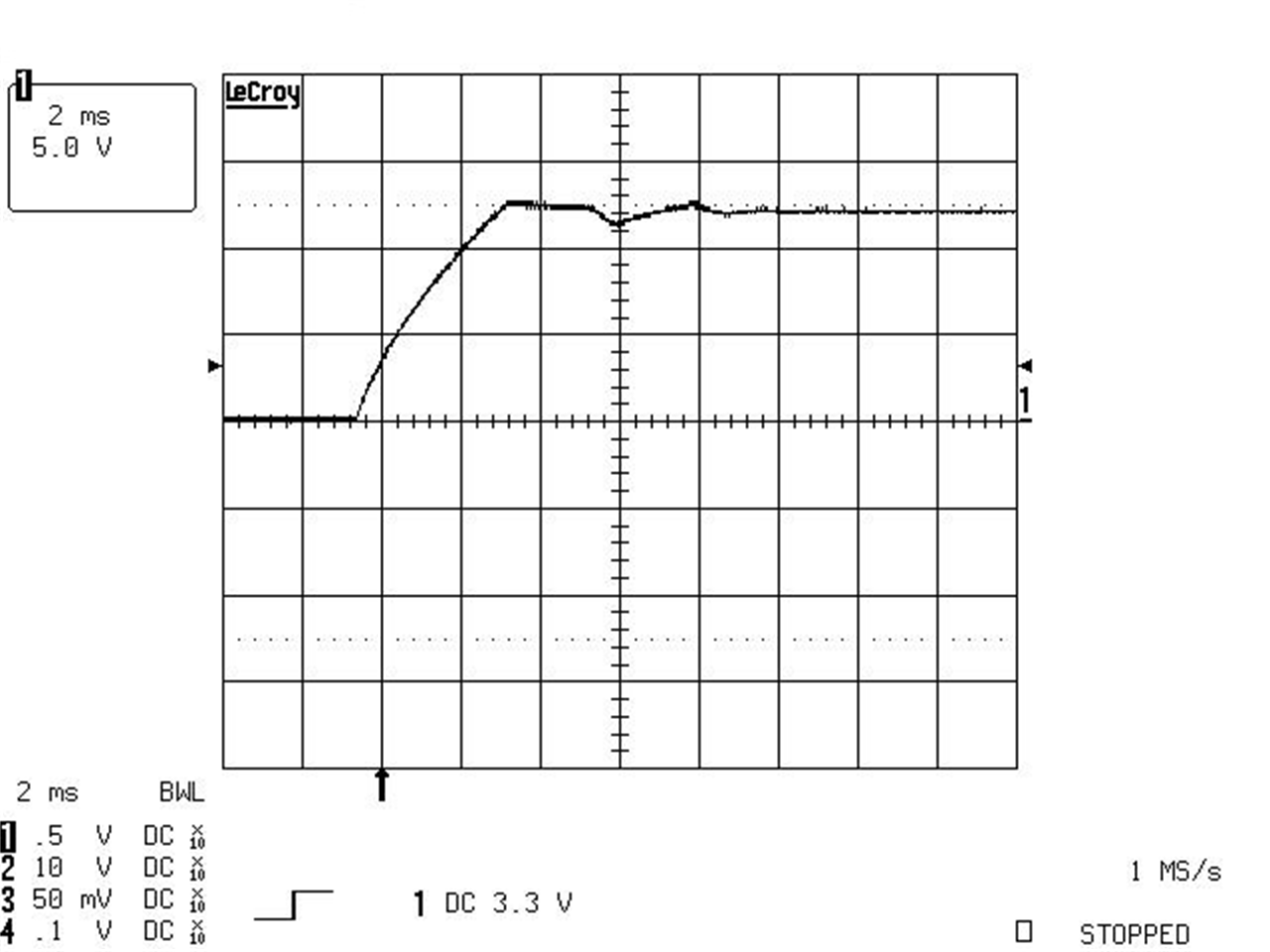
GUID-62965983-5D39-4830-86F6-160BABEB92AC-low.pngFigure 9-11 Output Voltage Behavior at Full Load Start-up (5 V/div)
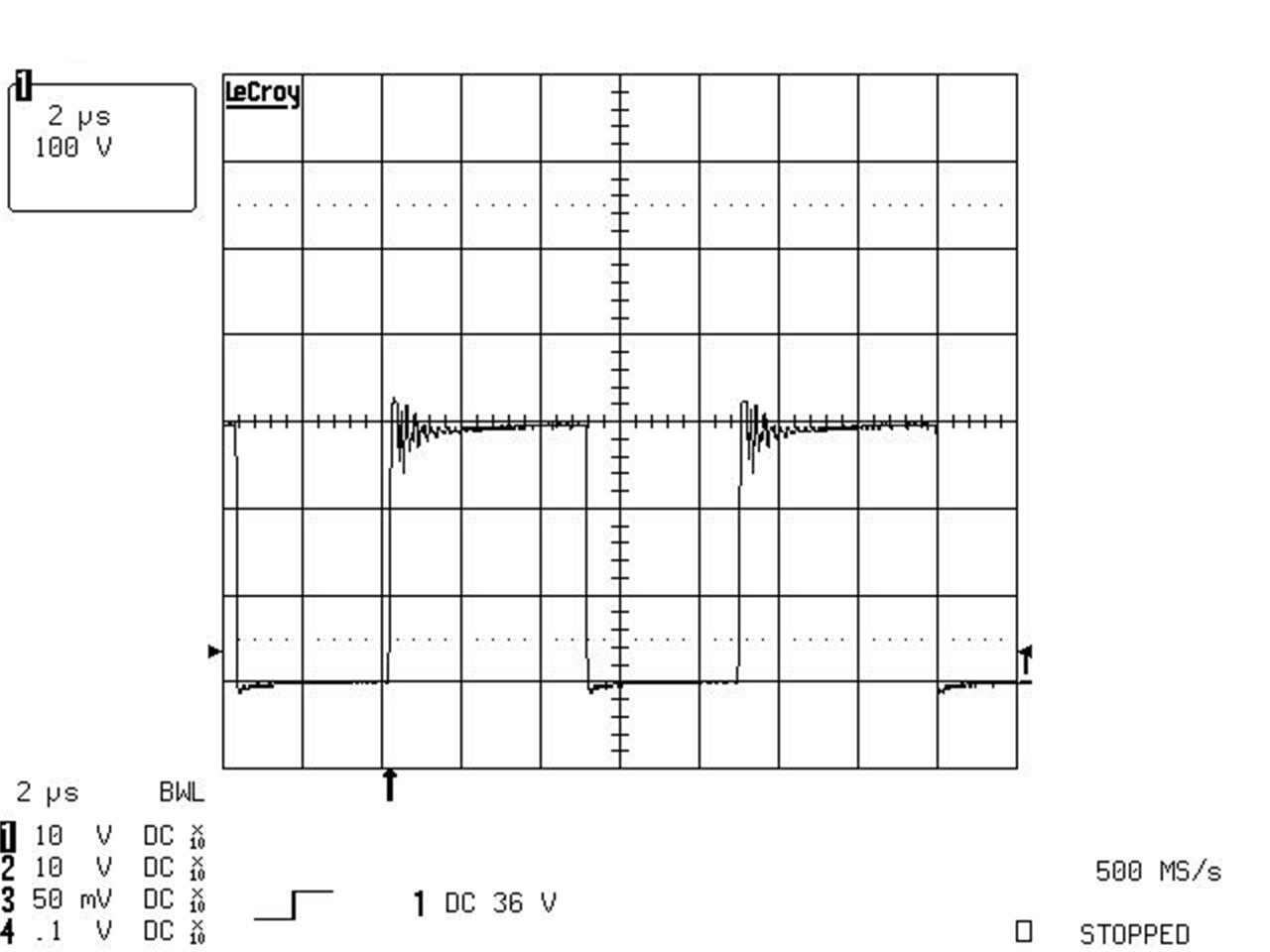
GUID-42D75AAC-E347-456A-B733-275A4CC8891C-low.pngFigure 9-8 Primary Side MOSFET Drain to Source Voltage at 120-V AC Input (100 V/div)
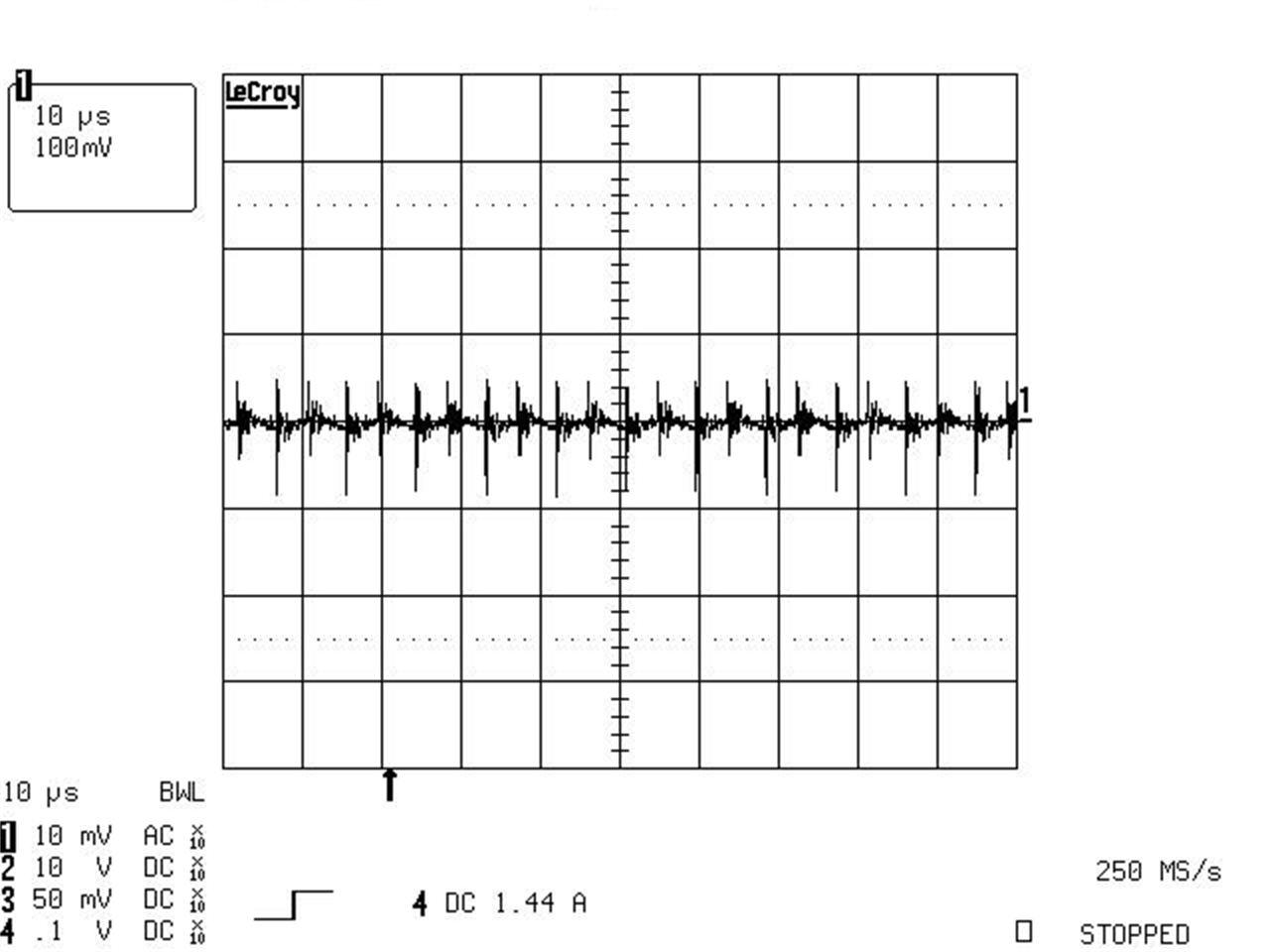
GUID-4D042F9D-EC29-4FAF-BB5C-33998E89F606-low.png
Figure 9-10 Output Voltage Ripple at Full Load (100 mV/div)