SLUSA12G December 2009 – November 2022 UCC28C40-Q1 , UCC28C41-Q1 , UCC28C42-Q1 , UCC28C43-Q1 , UCC28C44-Q1 , UCC28C45-Q1
PRODUCTION DATA
- 1 Features
- 2 Applications
- 3 Description
- 4 Revision History
- 5 Device Comparison Table
- 6 Pin Configuration and Functions
- 7 Specifications
-
8 Detailed Description
- 8.1 Overview
- 8.2 Functional Block Diagram
- 8.3 Feature Description
- 8.4 Device Functional Modes
-
9 Application and Implementation
- 9.1 Application Information
- 9.2
Typical Application
- 9.2.1 Design Requirements
- 9.2.2
Detailed Design Procedure
- 9.2.2.1 Custom Design With WEBENCH® Tools
- 9.2.2.2 Input Bulk Capacitor and Minimum Bulk Voltage
- 9.2.2.3 Transformer Turns Ratio and Maximum Duty CycleG
- 9.2.2.4 Transformer Inductance and Peak Currents
- 9.2.2.5 Output Capacitor
- 9.2.2.6 Current Sensing Network
- 9.2.2.7 Gate Drive Resistor
- 9.2.2.8 VREF Capacitor
- 9.2.2.9 RT/CT
- 9.2.2.10 Start-Up Circuit
- 9.2.2.11 Voltage Feedback Compensation
- 9.2.3 Application Curves
- 9.2.4 Power Supply Recommendations
- 9.2.5 Layout
- 10Device and Documentation Support
- 11Mechanical, Packaging, and Orderable Information
Package Options
Mechanical Data (Package|Pins)
- D|8
Thermal pad, mechanical data (Package|Pins)
Orderable Information
8.3.9 Slope Compensation
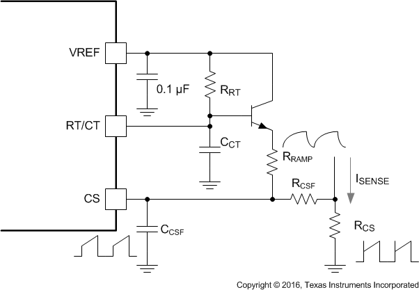
With current mode control, slope compensation is required to stabilize the overall loop with duty cycles exceeding 50%. Although not required, slope compensation also improves stability in applications using below a 50% maximum duty cycle. Slope compensation is introduced by injecting a portion of the oscillator waveform to the actual sensed primary current. The two signals are summed together at the current sense input (CS) connection at the filter capacitor. To minimize loading on the oscillator, it is best to buffer the timing capacitor waveform with a small transistor whose collector is connected to the reference voltage.
 Figure 8-8 Slope Compensation Circuit