JAJSJG6A december   2021  – june 2023 TDP0604

PRODUCTION DATA  

  1.   1
  2. 特長
  3. アプリケーション
  4. 概要
  5. Revision History
  6. Pin Configuration and Functions
  7. Specifications
    1. 6.1 Absolute Maximum Ratings
    2. 6.2 ESD Ratings
    3. 6.3 Recommended Operating Conditions
    4. 6.4 Thermal Information
    5. 6.5 Electrical Characteristics
    6. 6.6 Timing Requirements
    7. 6.7 Switching Characteristics
    8. 6.8 Typical Characteristics
    9. 6.9 Typical Characteristics
  8. Parameter Measurement Information
  9. Detailed Description
    1. 8.1 Overview
    2. 8.2 Functional Block Diagram
    3. 8.3 Feature Description
      1. 8.3.1  4-Level Inputs
      2. 8.3.2  I/O Voltage Level Selection
      3. 8.3.3  HPD_OUT
      4. 8.3.4  Lane Control
      5. 8.3.5  Swap
      6. 8.3.6  Linear and Limited Redriver
      7. 8.3.7  Main Link Inputs
      8. 8.3.8  Receiver Equalizer
      9. 8.3.9  CTLE Bypass
      10. 8.3.10 Input Signal Detect
      11. 8.3.11 Main Link Outputs
        1. 8.3.11.1 Transmitter Bias
        2. 8.3.11.2 Transmitter Impedance Control
        3. 8.3.11.3 TX Slew Rate Control
        4. 8.3.11.4 TX Pre-Emphasis and De-Emphasis Control
        5. 8.3.11.5 TX Swing Control
      12. 8.3.12 DDC Buffer
      13. 8.3.13 HDMI DDC Capacitance
      14. 8.3.14 DisplayPort
    4. 8.4 Device Functional Modes
      1. 8.4.1 MODE Control
        1. 8.4.1.1 I2C Mode (MODE = "F")
        2. 8.4.1.2 Pin Strap Modes
          1. 8.4.1.2.1 Pin-Strap: HDMI 1.4 and HDMI 2.0 Functional Description
      2. 8.4.2 DDC Snoop Feature
        1. 8.4.2.1 HDMI Type
      3. 8.4.3 Low Power Modes
    5. 8.5 Programming
      1. 8.5.1 Pseudocode Examples
        1. 8.5.1.1 HDMI 2.0 Source Example with DDC Snoop and DDC Buffer Enabled
      2. 8.5.2 TDP0604 I2C Address Options
      3. 8.5.3 I2C Target Behavior
    6. 8.6 Register Maps
      1. 8.6.1 TDP0604 Registers
  10. Application and Implementation
    1. 9.1 Application Information
    2. 9.2 Typical Source-Side Application
      1. 9.2.1 Design Requirements
      2. 9.2.2 Detailed Design Procedure
        1. 9.2.2.1 Pre-Channel (LAB)
        2. 9.2.2.2 Post-Channel (LCD)
        3. 9.2.2.3 Common Mode Choke
        4. 9.2.2.4 ESD Protection
      3. 9.2.3 Application Curves
    3. 9.3 Power Supply Recommendations
      1. 9.3.1 Supply Decoupling
    4. 9.4 Layout
      1. 9.4.1 Layout Guidelines
      2. 9.4.2 Layout Example
  11. 10Device and Documentation Support
    1. 10.1 Documentation Support
      1. 10.1.1 Related Documentation
    2. 10.2 ドキュメントの更新通知を受け取る方法
    3. 10.3 サポート・リソース
    4. 10.4 Trademarks
    5. 10.5 静電気放電に関する注意事項
    6. 10.6 用語集
  12. 11Mechanical, Packaging, and Orderable Information

パッケージ・オプション

メカニカル・データ(パッケージ|ピン)
サーマルパッド・メカニカル・データ
発注情報

Swap

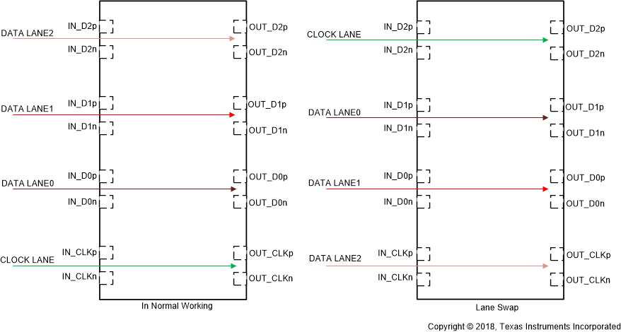
Figure 8-1 shows how TDP0604 incorporates a swap function which can swap the lanes. The RX EQ, pre-emphasis, termination, and slew configurations will follow the new mapping. This function is supported in pin strap mode as well as when TDP0604 is configured for I2C mode. A register controls the swap function in I2C mode.

Table 8-3 Swap Functions
Normal Operation
CFG1 pin = L or LANE_SWAP Register is 0h
CFG1 = H or LANE_SWAP Register is 1h
IN_D2 → OUT_D2IN_CLK → OUT_CLK
IN_D1 → OUT_D1IN_D0 → OUT_D0
IN_D0 → OUT_D0IN_D1 → OUT_D1
IN_CLK → OUT_CLKIN_D2 → OUT_D2
GUID-531C5778-E123-4F65-B9B0-C34BC3141C8D-low.gifFigure 8-1 TDP0604 Swap Function