JAJSNA0 December 2022 TPS25762-Q1
PRODUCTION DATA
- 1 特長
- 2 アプリケーション
- 3 概要
- 4 Revision History
- 5 Device Comparison Table
- 6 Pin Configuration and Functions
-
7 Specifications
- 7.1 Absolute Maximum Ratings
- 7.2 ESD Ratings
- 7.3 Recommended Operating Conditions
- 7.4 Recommended Components
- 7.5 Thermal Information
- 7.6 Buck-Boost Regulator
- 7.7 CC Cable Detection Parameters
- 7.8 CC VCONN Parameters
- 7.9 CC PHY Parameters
- 7.10 Thermal Shutdown Characteristics
- 7.11 Oscillator Characteristics
- 7.12 ADC Characteristics
- 7.13 TVS Parameters
- 7.14 Input/Output (I/O) Characteristics
- 7.15 BC1.2 Characteristics
- 7.16 I2C Requirements and Characteristics
- 7.17 Typical Characteristics
- 8 Parameter Measurement Information
-
9 Detailed Description
- 9.1 Overview
- 9.2 Functional Block Diagram
- 9.3
Feature Description
- 9.3.1 Device Power Management and Supervisory Circuitry
- 9.3.2 TVSP Device Configuration and ESD Protection
- 9.3.3
Buck-Boost Regulator
- 9.3.3.1 Buck-Boost Regulator Operation
- 9.3.3.2 Switching Frequency, Frequency Dither, Phase-Shift and Synchronization
- 9.3.3.3 VIN Supply and VIN Over-Voltage Protection
- 9.3.3.4 Feedback Paths and Error Amplifiers
- 9.3.3.5 Transconductors and Compensation
- 9.3.3.6 Output Voltage DAC, Soft-Start and Cable Droop Compensation
- 9.3.3.7 VBUS Overvoltage Protection
- 9.3.3.8 VBUS Undervoltage Protection
- 9.3.3.9 Current Sense Resistor (RSNS) and Current Limit Operation
- 9.3.3.10 Buck-Boost Peak Current Limits
- 9.3.4 USB-PD Physical Layer
- 9.3.5 VCONN
- 9.3.6 Cable Plug and Orientation Detection
- 9.3.7 ADC
- 9.3.8 BC 1.2, Legacy and Fast Charging Modes (Px_DP, Px_DM)
- 9.3.9 USB2.0 Low-Speed Endpoint
- 9.3.10 Digital Interfaces
- 9.3.11 I2C Interface
- 9.3.12 Digital Core
- 9.3.13 NTC Input
- 9.3.14 Thermal Sensors and Thermal Shutdown
- 9.4 Device Functional Modes
- 10Application and Implementation
- 11Power Supply Recommendations
- 12Layout
- 13Device and Documentation Support
- 14Mechanical, Packaging, and Orderable Information
10.2.2.5 Inductor Currents
Table 10-1 lists recommended inductor values based on desired switching frequency, fSW. The following equations were used to derive the values in the Buck Calculation and Boost Calculation results tables below.
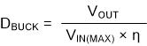
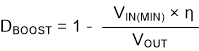
where
- VIN(MAX) = maximum input voltage
- VIN(MIN) = minimum input voltage
- VOUT = output voltage
- DBUCK = minimum duty cycle for buck mode
- DBOOST = maximum duty cycle for boost mode
- η = estimated efficiency calculated at VIN, VOUT, and IOUT
Buck Mode
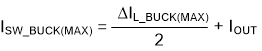

where
- VIN(MAX) = maximum input voltage
- VOUT(MIN) = minimum output voltage
- IOUT = maximum DC output current
- ΔIL-BUCK(MAX) = maximum ripple current through the inductor when in buck operation
- ISW_BUCK(MAX) = maximum switch current when in buck operation
- DBUCK = minimum duty cycle for buck operation
- fSW = switching frequency of the converter
- L = selected inductor value
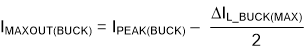
where
- IMAXOUT(BUCK) = maximum deliverable current through inductor by the converter
- IPEAK(BUCK) = buck switch peak current limit from Electrical Characteristics table
- ΔIL_BUCK(MAX) = Ripple current through the inductor calculated in Equation 14.
Boost Mode

where
- VIN(MIN) = minimum input voltage
- VOUT(MAX) = desired output voltage
- IOUT = desired output current
- ΔIL_BOOST(MAX) = maximum ripple current through the inductor in boost operation
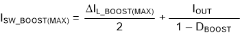
- ISW_BOOST(MAX) = maximum switch current in boost operation
- DBOOST = maximum duty cycle for boost operation
- fSW= switching frequency of the converter
- L = selected inductor value
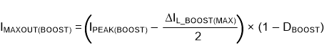
where
- IMAXOUT(BOOST) = maximum deliverable current through inductor by the converter
- DBOOST = maximum duty cycle for boost mode
- IPEAK(BOOST) = boost switch peak current limit from from Electrical Characteristics table
- ΔIL_MAX(BOOST) = Ripple current through the inductor calculated in Equation 17.
Buck Operation
Table 10-6 provides the tabulated ΔIL_BUCK(MAX) and ISW_BUCK(MAX) for the conditions below.
- η = 0.95
- VIN(MAX) = 18 V
- VOUT(MIN) = 3.3 V
- DBUCK(MIN) = 0.193
| fSW (kHz) |
IOUT (A) |
ΔIL_BUCK(MAX) (A) |
ISW_BUCK(MAX) (A) |
|---|---|---|---|
| 300 | 3.00 | 2.87 | 4.44 |
| 400 | 3.00 | 2.15 | 4.08 |
| 450 | 3.00 | 1.91 | 3.96 |
| 300 | 3.00 | 2.01 | 4.01 |
| 400 | 3.00 | 1.51 | 3.76 |
| 450 | 3.00 | 1.34 | 3.67 |
Boost Operation
Table 10-7 provides the tabulated ΔIL_BOOST(MAX), ISW_BOOST(MAX), suggested GUI IPEAK(BOOST) (MIN) settings for the maximum output power conditions shown below.
If ISW_BOOST(MAX) > IPEAK(BOOST) (MIN) → VBUS dropout likely.
If ISW_BOOST(MAX) < IPEAK(BOOST) (MIN) → VBUS regulates normally.
- η = 0.95
- VIN(MIN) = 5.5 V to 9 V
- VOUT(MAX) = 21 V
- IOUT = 3 A
To be noted, the calculation here uses 21V 3 A instead of 20 V 3.25A because 21 V 3A has bigger inductor peak current.
| fSW (kHz) |
VIN(MIN) (V) |
DBOOST(MAX) | ΔIL_BOOST(MAX) (A) |
ISW_BOOST(MAX) (A) |
GUI (1) IPEAK(BOOST) (A) |
|---|---|---|---|---|---|
| 300 | 5.5 | 0.751 | 2.93 | 13.51 | 12.3 |
| 6 | 0.729 | 3.10 | 12.62 | 12.3 | |
| 6.5 | 0.706 | 3.25 | 11.83 | 12.3 | |
| 7 | 0.683 | 3.39 | 11.16 | 12.3 | |
| 7.5 | 0.661 | 3.52 | 10.61 | 10.8 | |
| 8 | 0.638 | 3.62 | 10.10 | 10.8 | |
| 8.5 | 0.615 | 3.71 | 9.65 | 10.8 | |
| 9 | 0.593 | 3.79 | 9.27 | 9.3 | |
| 400 | 5.5 | 0.751 | 2.20 | 13.15 | 12.3 |
| 6 | 0.729 | 2.33 | 12.24 | 12.3 | |
| 6.5 | 0.706 | 2.44 | 11.42 | 12.3 | |
| 7 | 0.683 | 2.54 | 10.73 | 10.8 | |
| 7.5 | 0.661 | 2.64 | 10.17 | 10.8 | |
| 8 | 0.638 | 2.71 | 9.64 | 10.8 | |
| 8.5 | 0.615 | 2.78 | 9.18 | 9.3 | |
| 9 | 0.593 | 2.84 | 8.79 | 9.3 | |
| 450 | 5.5 | 0.751 | 1.95 | 13.02 | 12.3 |
| 6 | 0.729 | 2.07 | 12.11 | 12.3 | |
| 6.5 | 0.706 | 2.17 | 11.29 | 12.3 | |
| 7 | 0.683 | 2.26 | 10.59 | 10.8 | |
| 7.5 | 0.661 | 2.34 | 10.02 | 10.8 | |
| 8 | 0.638 | 2.41 | 9.49 | 9.3 | |
| 8.5 | 0.615 | 2.47 | 9.03 | 9.3 | |
| 9 | 0.593 | 2.51 | 8.63 | 9.3 |