JAJSNA0 December 2022 TPS25762-Q1
PRODUCTION DATA
- 1 特長
- 2 アプリケーション
- 3 概要
- 4 Revision History
- 5 Device Comparison Table
- 6 Pin Configuration and Functions
-
7 Specifications
- 7.1 Absolute Maximum Ratings
- 7.2 ESD Ratings
- 7.3 Recommended Operating Conditions
- 7.4 Recommended Components
- 7.5 Thermal Information
- 7.6 Buck-Boost Regulator
- 7.7 CC Cable Detection Parameters
- 7.8 CC VCONN Parameters
- 7.9 CC PHY Parameters
- 7.10 Thermal Shutdown Characteristics
- 7.11 Oscillator Characteristics
- 7.12 ADC Characteristics
- 7.13 TVS Parameters
- 7.14 Input/Output (I/O) Characteristics
- 7.15 BC1.2 Characteristics
- 7.16 I2C Requirements and Characteristics
- 7.17 Typical Characteristics
- 8 Parameter Measurement Information
-
9 Detailed Description
- 9.1 Overview
- 9.2 Functional Block Diagram
- 9.3
Feature Description
- 9.3.1 Device Power Management and Supervisory Circuitry
- 9.3.2 TVSP Device Configuration and ESD Protection
- 9.3.3
Buck-Boost Regulator
- 9.3.3.1 Buck-Boost Regulator Operation
- 9.3.3.2 Switching Frequency, Frequency Dither, Phase-Shift and Synchronization
- 9.3.3.3 VIN Supply and VIN Over-Voltage Protection
- 9.3.3.4 Feedback Paths and Error Amplifiers
- 9.3.3.5 Transconductors and Compensation
- 9.3.3.6 Output Voltage DAC, Soft-Start and Cable Droop Compensation
- 9.3.3.7 VBUS Overvoltage Protection
- 9.3.3.8 VBUS Undervoltage Protection
- 9.3.3.9 Current Sense Resistor (RSNS) and Current Limit Operation
- 9.3.3.10 Buck-Boost Peak Current Limits
- 9.3.4 USB-PD Physical Layer
- 9.3.5 VCONN
- 9.3.6 Cable Plug and Orientation Detection
- 9.3.7 ADC
- 9.3.8 BC 1.2, Legacy and Fast Charging Modes (Px_DP, Px_DM)
- 9.3.9 USB2.0 Low-Speed Endpoint
- 9.3.10 Digital Interfaces
- 9.3.11 I2C Interface
- 9.3.12 Digital Core
- 9.3.13 NTC Input
- 9.3.14 Thermal Sensors and Thermal Shutdown
- 9.4 Device Functional Modes
- 10Application and Implementation
- 11Power Supply Recommendations
- 12Layout
- 13Device and Documentation Support
- 14Mechanical, Packaging, and Orderable Information
9.3.1.2 Internal LDO Regulators
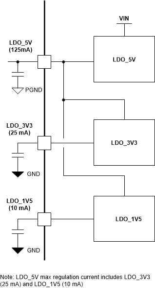
Three internal LDOs provide regulated supplies for operation of internal circuitry.
- LDO_5V: Supplies buck-boost gate drive circuitry, LDO_3V3, LDO_1V5, and PA and
PB VCONN power paths. External bypass capacitance, CLDO_5V is required for
proper operation. It is highly recommended to include an additional high frequency 0.1
μF capacitor in parallel with CLDO_5V. CLDO_5V and the parallel
high frequency should be placed as close to the LDO_5V pin as possible. This
capacitance: 1) provides energy storage for the buck-boost internal FET gate drivers,
and 2) is required to stabilize the internal 5-V LDO in applications where an external
5-V supply is not connected. The TPS25762-Q1 will not operate (release reset) until
VLDO_5V(UVLO_R) threshold is met. Hard reset occurs when VLDO_5V
< VLDO_5V(UVLO_F) threshold. Current from LDO_5V returns to PGND pin. The
LDO_5V output may be used to supply a small external loads such as indicator LEDs. When
supplying external components, it is recommended that the total external load current
not exceed 25 mA (MAX).
- 0.1W VCONN: when enabled in the application configuration GUI, LDO_5V is capable of sourcing 20 mA each to PA_VCONN and PB_VCONN.
- 1W VCONN: when enabled in the application configuration GUI, this mode of operation requires an external 4.75 - 5.5 V, 500-mA capable supply connected to LDO_5V. Back-feeding of LDO_5V is allowed.
- LDO_3V3: Supplies internal analog circuits, GPIO buffers, USB PD and the USB Endpoint PHYs. External bypass capacitance of CLDO_3V3 is required for proper operation. An additional 0.1 μF capacitor in parallel with CLDO_3V3 is highly recommended to filter high frequency noise from the I/O buffers and PHYs. The LDO_3V3 can supply external circuits at up to 25 mA. Expected loads include: EEPROM (5mA), NTC resistor divider network (< 1 mA). Current may be drawn up to ILDO_3V3(ILIMIT). Note: the USB PD and Endpoint PHYs draw current from LDO_3V3. If a CCx or Dx pin is shorted to GND during a transmission the current drawn may reach the current limit threshold. Similarly, if any GPIO pins are configured as push-pull outputs and a GPIO short to GND event occurs, the LDO_3V3 current limit may be reached. Current returns to AGND pin.
- LDO_1V5: Supplies digital core. External bypass capacitance of CLDO_1V5 is required for proper operation. An additional 0.1 μF capacitor in parallel with CLDO_1V5 is highly recommended to filter noise generated by the digital core. The M0 is held in reset until all three UVLO_R (rising) thresholds are met. Current returns to AGND pin.
 Figure 9-3 Internal LDO Connection
Diagram