SCDA008C June 2021 – November 2021 CD4052B , TS3A225E , TS3A44159
- Trademarks
- 1Introduction
- 2Semiconductor Switches
- 3Basic Signal-Switch Structures
- 4Key Concerns in Digital-Switch Applications
- 5Signal Switch Families
- 6Applications
- 7Conclusion
- 8References
- 9Revision History
-
A Test
Measurement Circuits
- A.1 Measurement Setup for ron
- A.2 Measurement Setup for VO vs VI Characteristics
- A.3 Voltage-Time Waveform Measurement (Switch On)
- A.4 Voltage-Time Waveform Measurement (Switch Off)
- A.5 Output-Skew Measurement
- A.6 Simulation Setup for Undershoot Measurement
- A.7 Laboratory Setup for Attenuation Measurement
- A.8 Laboratory Setup for Off Isolation Measurement
- A.9 Laboratory Setup for Crosstalk Measurement
4.1 Power and Control Voltage Requirements
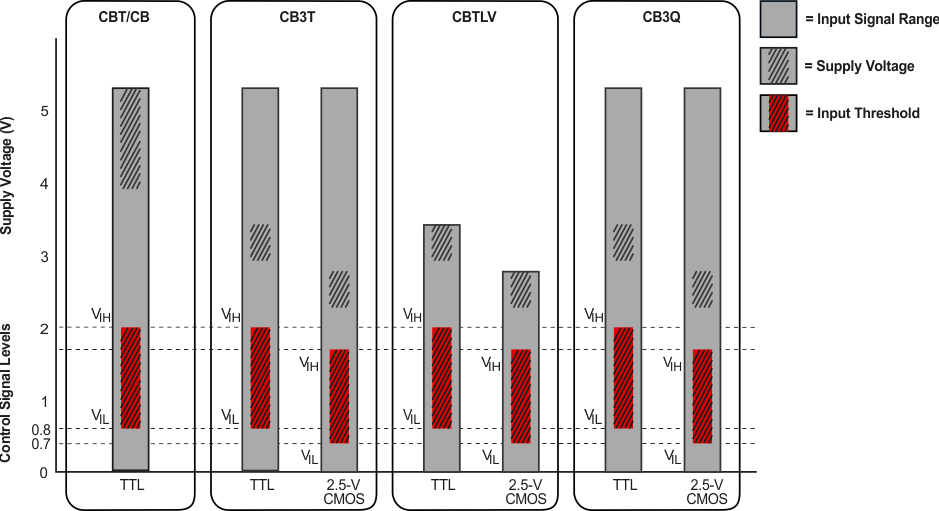
One of the first considerations that must be made when selecting a switch is the supply rail voltage and the allowable input range of the signals passed through the switch. As shown in Figure 4-1, the CBT/CBT-C family of devices supports 5 V supply rails, while the CB3T, CBTLV, and CB3Q families support 2.5 V and 3.3 V rails. The dark blue regions indicate the voltage range of signals that are able to be passed through the switch. In some cases, these ranges match the supply voltage (CBT/CBT-C and CBTLV), while other switch families may pass signals that extend beyond the supply rail (CB3T and CB3Q). System requirements may dictate which devices can be used in a particular application. For example, designs implementing a 5 V supply rail and a 5 V signal are likely best served by a device in the CBT/CBT-C family, while a design using a 3.3 V supply rail and a 4 V signal are best served by a device in the CB3T or CB3Q family.
 Figure 4-1 Control Signal Levels (VIH, VIL) and Supply Voltage
The input thresholds of these devices allow users to implement 3.3 V logic or 5 V logic, regardless of the supply voltage or signal voltage being used in design. The red bars in Figure 4-1 show the logic level voltage thresholds for the different digital switch families.