SCDA008C June 2021 – November 2021 CD4052B , TS3A225E , TS3A44159
- Trademarks
- 1Introduction
- 2Semiconductor Switches
- 3Basic Signal-Switch Structures
- 4Key Concerns in Digital-Switch Applications
- 5Signal Switch Families
- 6Applications
- 7Conclusion
- 8References
- 9Revision History
-
A Test
Measurement Circuits
- A.1 Measurement Setup for ron
- A.2 Measurement Setup for VO vs VI Characteristics
- A.3 Voltage-Time Waveform Measurement (Switch On)
- A.4 Voltage-Time Waveform Measurement (Switch Off)
- A.5 Output-Skew Measurement
- A.6 Simulation Setup for Undershoot Measurement
- A.7 Laboratory Setup for Attenuation Measurement
- A.8 Laboratory Setup for Off Isolation Measurement
- A.9 Laboratory Setup for Crosstalk Measurement
5.1 CBT-C Family
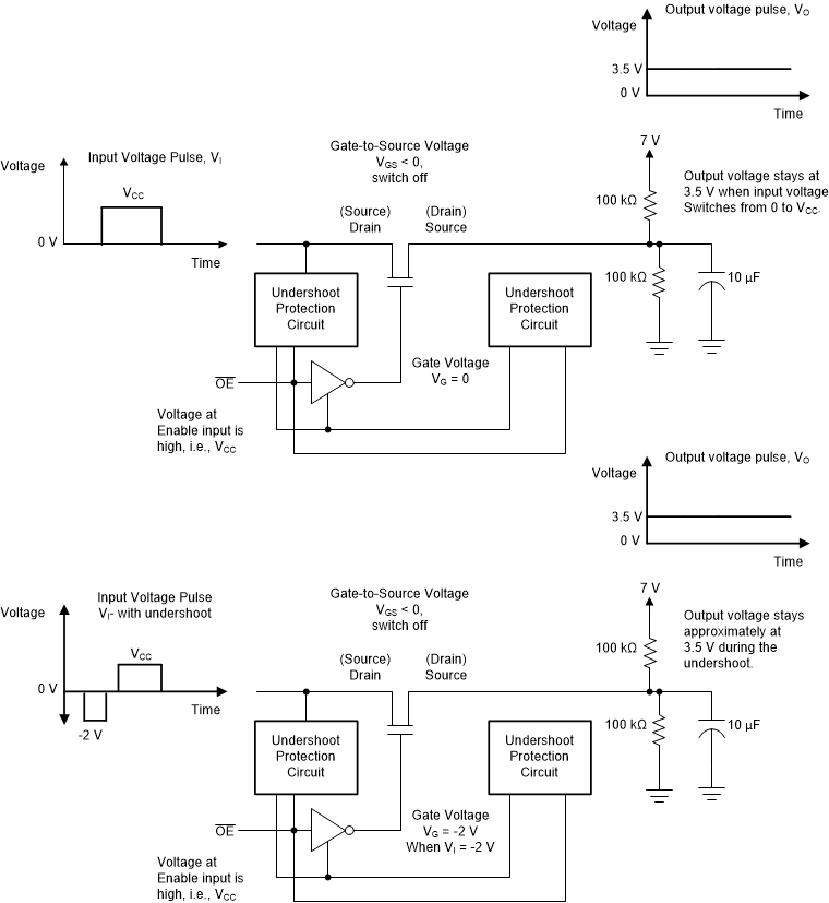
The switches in the CBT-C (Cross-Bar Technology - Clamp) family are NMOS series switches. The operating VCC of this family is 5 V, and switching for various standards (for example, LVCMOS, LVTTL, and so forth) can be accomplished. This family also has an undershoot protection circuit integrated in the bus switch. The undershoot protection circuit prevents the n-channel pass transistor from turning on when the switch is off. When undershoot occurs, this circuit senses the negative voltage at the input and biases the gate of the n-channel pass transistor to that negative voltage. Since the gate and source voltage are now at the same potential (<0 V), the switch remains off. Undershoot protection on one side of the off switch can prevent up to –2 V undershoots on the other side of the switch. Static power consumption of this family is negligible. Dynamic power consumption depends on the frequency of the enable input of the device. Switching high and low at the enable input causes internal CMOS inverters to switch between low and high; therefore, a higher frequency of the control input signal results in higher dynamic power consumption. Undershoot protection in CBT-C is shown in Figure 5-1.
 Figure 5-1 Undershoot Protection in CBT-C When Enable Input (OE) Voltage is High