SLVA888C April 2017 – January 2021 TPS65987D , TPS65988
- Trademarks
- 1Schematic Design Guidelines
- 2Layout Guidelines
- 3Summary
- 4References
- A Appendix
- Revision History
2.3 Other Considerations
This section covers other design considerations such as placement of components and other best practices to be followed.
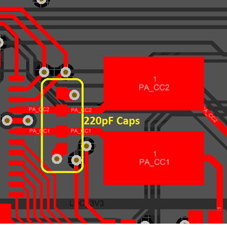
- Try to reduce the distance between the Type-C receptacle and the CC pins of the PD Controller. Place the 220-pF capacitor close to the PD Controller. The capacitors on the CC lines help to tune the eye-diagram of CC signals.
- Place ESD diodes as close as possible to the Type-C receptacle.
- The ESD components must be placed without stubs in a pass through manner on the differential path.
- Keep all the power regulators away from the high speed signals and associated components.
 Figure 2-3 Placement of Capacitors on CC Lines