SLVA888C April 2017 – January 2021 TPS65987D , TPS65988
- Trademarks
- 1Schematic Design Guidelines
- 2Layout Guidelines
- 3Summary
- 4References
- A Appendix
- Revision History
1.2.1 BUSPOWER (ADCIN1)
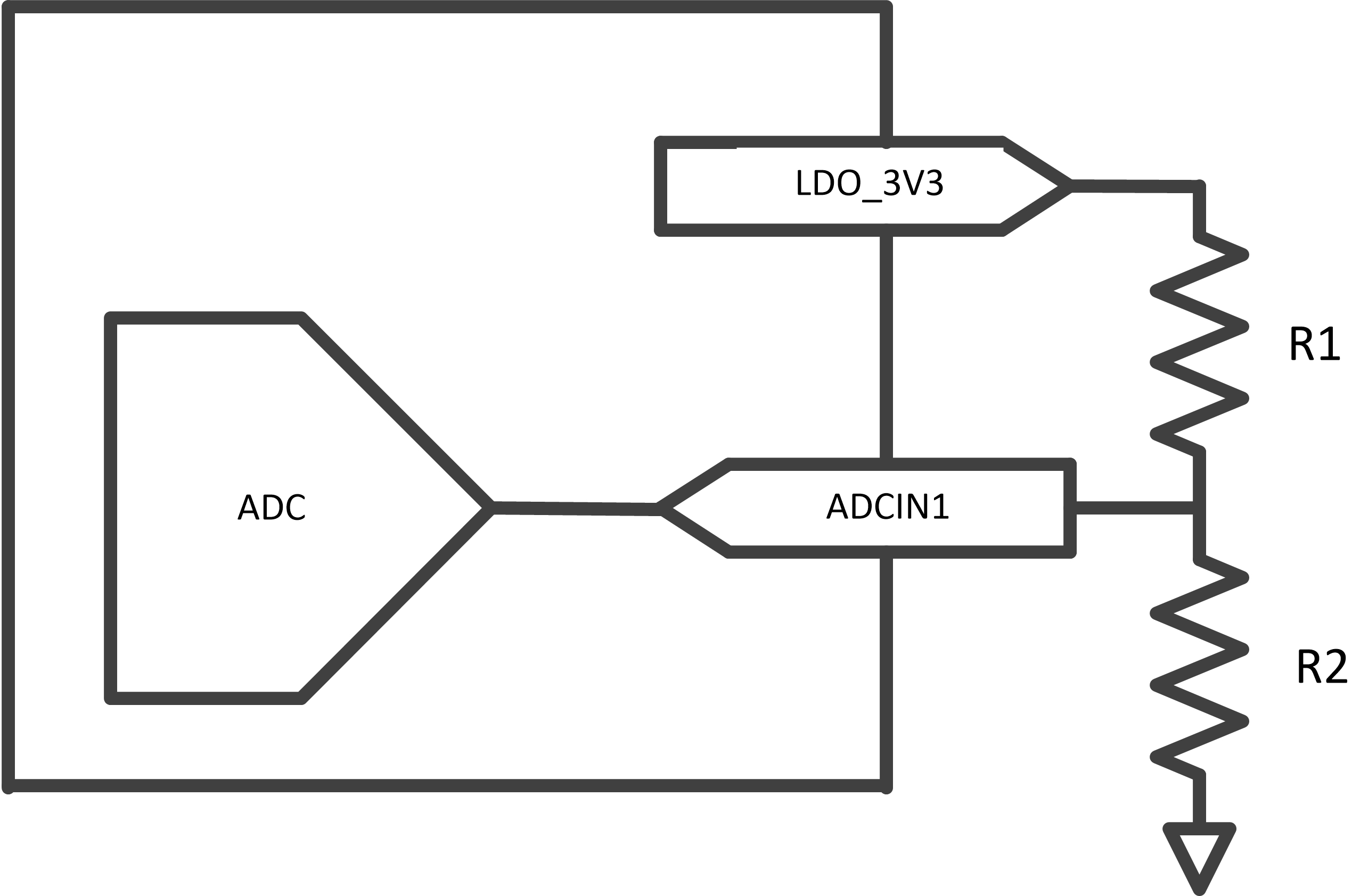
This pin is used for boot strap pin for device initialization. In dead battery operation, the chip voltage at the VBUS pin determines how the power is used. This pin along with the SPI_MISO pin with help to pick the right device configuration from the ROM. A potential divider should be used between LDO_3V3 and GND to pick the right configuration. Please refer the device data sheet for more information.
External resistor tolerance of 1% is required.
Do not connect ADCIN1 pin directly to Ground or LDO_3V3 rail. Use resistor divider as recommended in the data sheet.
 Figure 1-2 ADCIN1 Resistor Divider
Network