SLVA888C April 2017 – January 2021 TPS65987D , TPS65988
- Trademarks
- 1Schematic Design Guidelines
- 2Layout Guidelines
- 3Summary
- 4References
- A Appendix
- Revision History
1.3.1 I2C Pin Address Setting (ADCIN2)
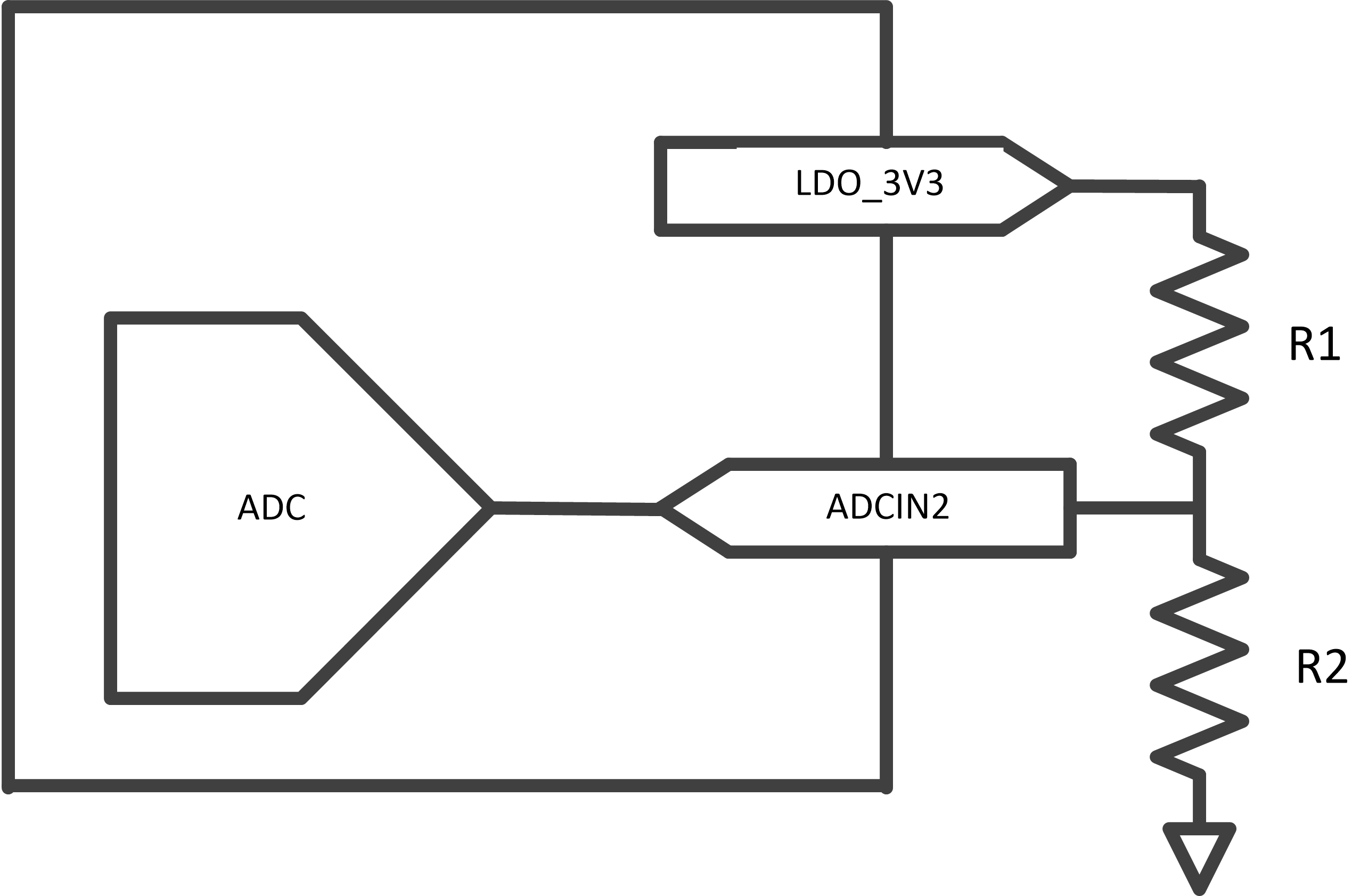
ADCIN2 pin is used to set the I2C address of the device. At boot time, the chip determines the voltage and sets the I2C address. A potential divider must be used between LDO_3V3 and GND to get the desired I2C address. I2C address of the I2C port 1 as per Table 1-2
 Figure 1-4 ADCIN2 Resistor Divided Network.
 Important: External resistor tolerance of 1% is required.
A potential divider must be used between LDO_3V3 and GND to get the desired I2C address. I2C address of the I2C port 1 as per Table 1-2.
Table 1-2 I2C Address of the I2C Port 1
| DIV = R2/(R1 + R2) | Default Unique Address I2C1 – Port1 (7-bit) | Default Unique Address I2C1 – Port2 | Resistor Recommendation | |
|---|---|---|---|---|
| DIV MIN | DIV MAX | |||
| Short ADCIN2 to GND | 0x20 | 0x24 | R2=100K | |
| 0.20 | 0.38 | 0x21 | 0x25 | R1=191K R2=100K |
| 0.40 | 0.58 | 0x22 | 0x26 | R1=100K R2=100K |
| Short ADCIN2 to LDO_3V3 | 0x23 | 0x27 | R1=100K | |