SPRAC76G November 2022 – February 2024 AM5706 , AM5708 , AM5716 , AM5718 , AM5726 , AM5728 , AM5729 , AM5746 , AM5748 , AM5749 , AM620-Q1 , AM623 , AM625 , AM625-Q1 , AM625SIP , AM6411 , AM6412 , AM6421 , AM6422 , AM6441 , AM6442 , AM6526 , AM6528 , AM6546 , AM6548
- 1
- Sitara Processor Power Distribution Networks: Implementation and Analysis
- Trademarks
- 1Introduction
- 2Guidelines for PCB Stack-Up
- 3Physical Layout Optimization of the PDN
- 4Static PDN Analysis (IR Drop Optimization)
- 5Dynamic Analysis of PCB PDN
- 6Checklist for PDN
- 7Implementation Examples and PDN Targets
- Revision History
3 Physical Layout Optimization of the PDN
The following are important requirements that need to be implemented in the PCB PDN design:
- External power trace routing between components should be as wide as possible as wider traces result in reduced DC resistance and consequently a lower static IR drop. They also provide for lower loop inductance and higher capacitance.
- Whenever possible, attempt to achieve a ratio of 1:1 (or better) for component pins and associated vias. Do not share vias among multiple capacitors.
- Placement of decoupling capacitors and associated vias should be as close to the processor ball as possible.
- The maximum current-carrying capacity of each transitional via should be evaluated through simulation to determine the appropriate number of vias required to connect components. This ensures that the current-carrying ability of a via interconnect network is sufficient for the needs of each particular component. When a via interconnect, or a network of same, is unable to supply sufficient current, this is referred to as “via starvation”.
- TI highly recommends that both static and dynamic IR drop analysis (discussed in Section 4 and Section 5) be performed on any new PCB design prior to fabrication. These analyses should be used to assess the appropriate number of vias and geometrical trace width dimensions required to meet the IR drop requirements of system components.
- Whenever possible for the internal layers (both signal routing and power plane), wide traces and copper area fills are recommended for PDN layout. As discussed in previous sections of this document, routing power nets in planes provides for more inter-plane capacitance and improves high frequency performance of the PDN.
- Decoupling capacitors should be mounted with minimum impact to inductance. A capacitor has characteristics not only of capacitance but also inductance and resistance. Figure 3-1 shows the parasitic model of a real capacitor. A real capacitor should be treated as an RLC circuit with effective series resistance (ESR) and effective series inductance (ESL).
 Figure 3-1 Characteristics of a “Real” Capacitor With ESL and ESR
The magnitude of the impedance of this series model is given in Equation 1.
Equation 1.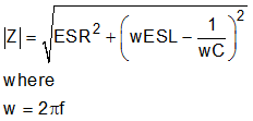
Figure 3-2 shows the resonant frequency response of a typical capacitor with self-resonant frequency of 55 MHz. The impedance of the capacitor is a combination of its series resistance and reactive capacitance and inductance as shown per Equation 1.
 Figure 3-2 Typical Impedance Profile of a Capacitor
 - Try to avoid different power nets coupling on the PCB by using “co-planar” shielding whenever appropriate. Figure 3-3 depicts an example of co-planar shielding for two different power nets (VDD_MPU_IVA and VDD_CORE).
 Figure 3-3 Example of “Co-Planar’ Shielding of Power Net Using Ground Guard-Band
As the capacitors have both series inductance and resistance that will impact their effectiveness, it is critical that the following recommendations are adopted in placing them on the power distribution network. Whenever possible make sure to mount the capacitor with the geometry that will minimize the mounting inductance and resistance. The capacitor mounting inductance and resistance includes the inductance and resistance of the pads, the trace, and the associated vias.
The length of a trace used to connect a capacitor has a significant impact on the parasitic inductance and resistance of the mounting. This trace should be as short and wide as possible. Wherever possible, minimize the trace by locating vias near the solder pad landing. Further improvements can be made to the mounting by placing vias to the side of capacitor lands or by doubling the number of vias. If the PCB manufacturing process allows, and if cost-effective, via-in-pad (VIP) geometries are strongly recommended.
The most common via placement geometries are proved below, in order of preference for reducing parasitic impact:
- Via-In-Pad (VIP)
- Dual Offset Via
- Single Offset Via
- Pad to Via Trace (short)
- Pad to Via Trace (long)
 Figure 3-4 Capacitor Mounting Geometries
In addition to mounting inductance and resistance associated with placing a capacitor on the PCB, the effectiveness of a decoupling capacitor also depends on the spreading inductance and resistance that the capacitor sees with respect to the load. The spreading inductance and resistance is strongly dependent on the layer assignment in the PCB stack-up (see Figure 2-1).