SPRAC76G November 2022 – February 2024 AM5706 , AM5708 , AM5716 , AM5718 , AM5726 , AM5728 , AM5729 , AM5746 , AM5748 , AM5749 , AM620-Q1 , AM623 , AM625 , AM625-Q1 , AM625SIP , AM6411 , AM6412 , AM6421 , AM6422 , AM6441 , AM6442 , AM6526 , AM6528 , AM6546 , AM6548
- 1
- Sitara Processor Power Distribution Networks: Implementation and Analysis
- Trademarks
- 1Introduction
- 2Guidelines for PCB Stack-Up
- 3Physical Layout Optimization of the PDN
- 4Static PDN Analysis (IR Drop Optimization)
- 5Dynamic Analysis of PCB PDN
- 6Checklist for PDN
- 7Implementation Examples and PDN Targets
- Revision History
4 Static PDN Analysis (IR Drop Optimization)
Delivering reliable power to circuits is always of critical importance as IR drops can occur at every level in a chip, package, and board system. Components that are distant from their associated power source are particularly susceptible to IR drop, and designs that rely on battery power must further minimize voltage drop to avoid unacceptable power loss. Early DC assessments made through simulation help to determine power distribution basics such as the best available entry point for power, layer stack-up choices, and estimates for the amount of copper needed to carry the required current.
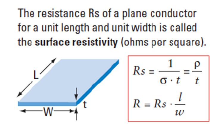
 Figure 4-1 Depiction of Sheet Resistivity
and Resistance
Figure 4-1 Depiction of Sheet Resistivity
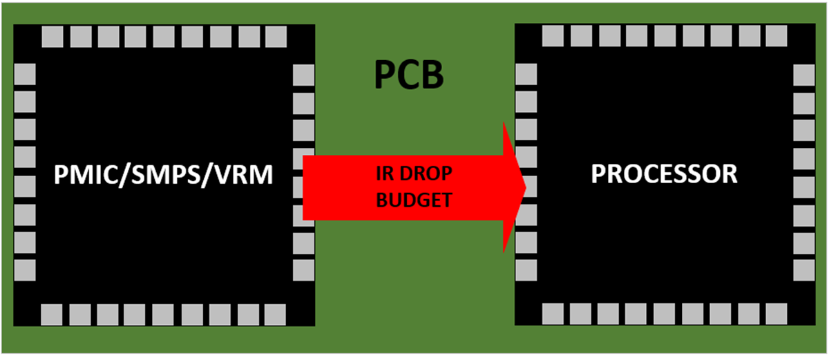
and ResistanceOhm’s Law (V=IR) relates conduction current to voltage drop, and at DC, the relation coefficient is a constant representing the resistance of the conductor. Conductors also dissipate power due to their resistance. Both voltage drop and power dissipation are proportional to the resistance of the conductor. Static IR or DC analysis/design methodology consists of designing the power distribution network such that the voltage drop (under DC operating conditions) across the power and ground pads of the application processor device is within a specified value of the nominal voltage to ensure proper functionality of the device. The PCB-level static IR drop budget is defined between the pins/pads of the power management device (PMIC/VRM/SMPS) and the BGA balls on the application processor device to which the power management device is supplying power (see Figure 4-2).
 Figure 4-2 PCB IR Drop Budget
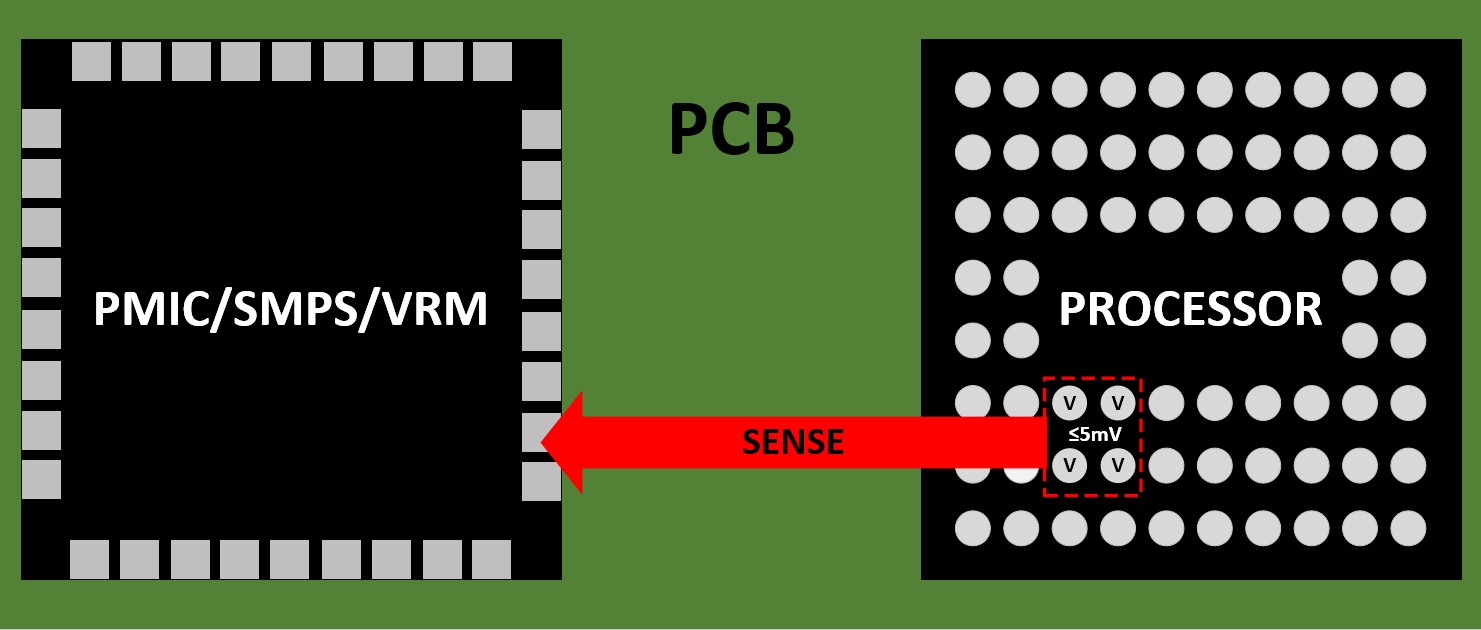
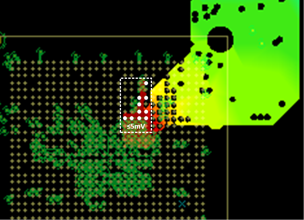
Given the total system-level margin allowed for proper device functionality, allowable voltage variation at the BGA of the device is typically specified at 2.5% of the nominal voltage. #T4815344-108(1)For devices implementing remote-sense functionality, it is a requirement that the power management device feedback/sense line(s) be placed as close to the relevant processor power balls as physically possible (see Figure 4-3) and that a supply input voltage difference of ≤5 mV under maximum current loading is maintained across all balls connected to a common power rail. This 5 mV maximum represents any voltage difference that may exist between a remote sense point and any associated power input (see Figure 4-4).
 Figure 4-3 Sense Line Placement
 Figure 4-4 Allowable Power Input Voltage
Difference