SPRAD62 February 2023 F29H850TU , F29H859TU-Q1 , TMS320F280023C , TMS320F280025C , TMS320F280025C-Q1 , TMS320F280037C , TMS320F280037C-Q1 , TMS320F280038C-Q1 , TMS320F280039C , TMS320F280039C-Q1 , TMS320F28386D , TMS320F28386D-Q1 , TMS320F28386S , TMS320F28386S-Q1 , TMS320F28388D , TMS320F28388S , TMS320F28P650DH , TMS320F28P650DK , TMS320F28P650SH , TMS320F28P650SK , TMS320F28P659DH-Q1 , TMS320F28P659DK-Q1 , TMS320F28P659SH-Q1
- Abstract
- Trademarks
- 1Introduction
- 2Serial Port Design Methodology
- 3Example A: Using the CLB to Input and Output a TDM Stream in Audio Applications
- 4Example B: Using the CLB to Implement a Custom Communication Bus for LED Driver in Lighting Applications
- 5References
4.6 Step 5: Simulate the Logic Design
A data receive operation is simulated in Figure 4-15. For this simulation a simple pattern of 0xAAAA is used as data input. The simulation shows the beginning of the frame indicated by the START bit, the capture of the full received word, and the verification of the CHECK bit.
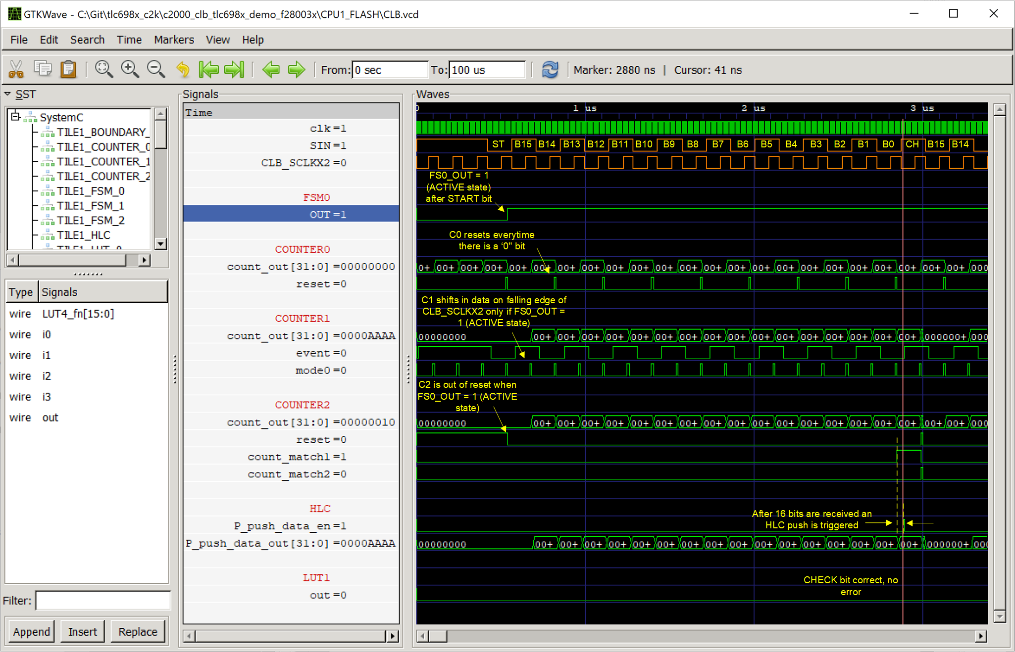 Figure 4-15 Data Receive Simulation for
LED Driver
Figure 4-15 Data Receive Simulation for
LED DriverA second data receive simulation is shown in Figure 4-16. In this simulation, an incorrect CHECK bit is added to the incoming data stream to verify the operation of the CHECK bit logic. The simulation shows the output of the LUT1 block go high to indicate a CHECK bit error is detected.
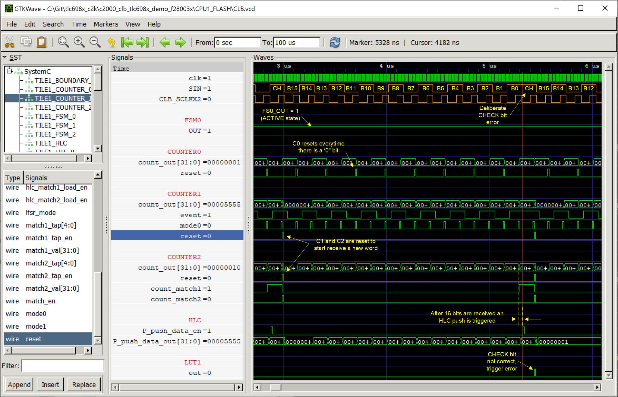 Figure 4-16 Check Bit Error Logic
Simulation
Figure 4-16 Check Bit Error Logic
SimulationFinally, the simulation in Figure 4-17 shows the detection of the END bits. The FSM0 block transitions the CLB logic to the IDLE state upon detection of the END bits.
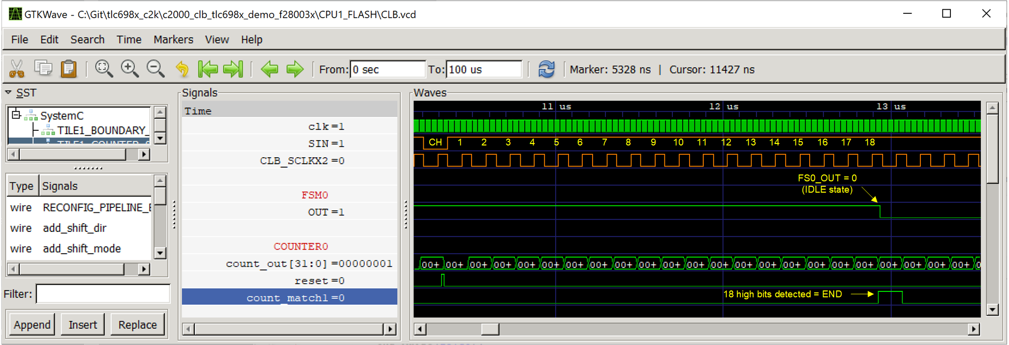 Figure 4-17 END Frame Detection
A data transmit operation is simulated in Figure 4-18. The simulation shows the transmission of a single 0x5555 word, starting from the START bit and ending with the END frame. To simplify the CLB logic, the START bit is implemented by allowing the tile to transmit a 0xFFFF word. The START bit is generated on the 17th clock cycle using the CHECK bit logic of the tile. Similarly, to generate the END frame, the CLB logic simply sets the CLB_SOUT signal to 1 at the end of the last word transmission. The CLB logic depends on the CPU to wait at least 18 PWM_SCLKX2 cycles before starting a new data transmission.
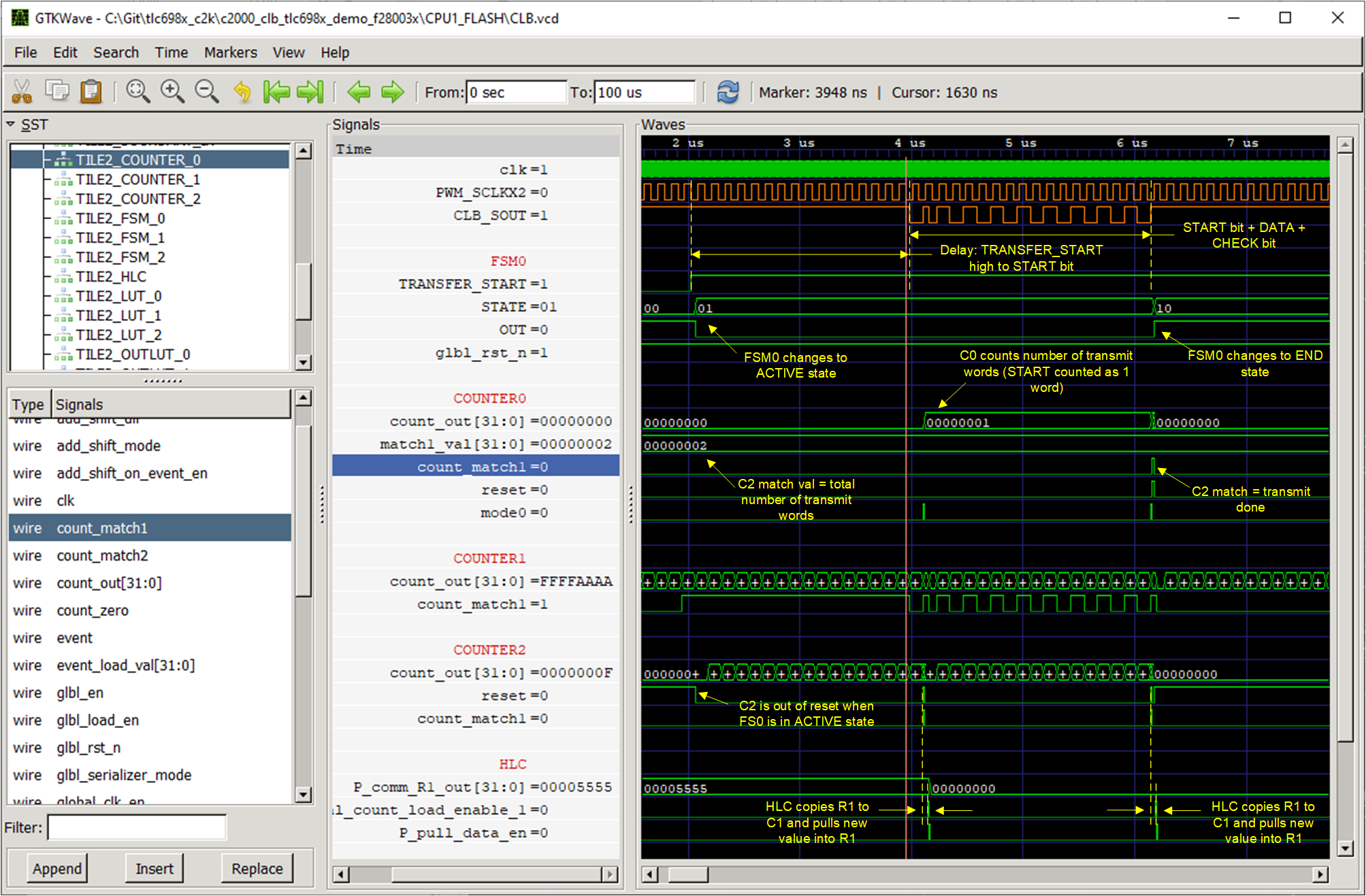 Figure 4-18 Data Transmit Simulation for
LED Driver
Figure 4-18 Data Transmit Simulation for
LED DriverAn output glitch is observed during data transmit operations due to the delay in updating the output serializer (Counter 1). Figure 4-19 shows the internal delays starting from the PWM_SCLKX2 low edge to the final update of the output serializer. The result of the glitch is a reduced setup time for the receiving device. The setup time should not be calculated from the rising edge of the PWM_SCLKX2 signal since this clock will also be delayed as it passes through the CLB tile. Instead, the setup time should be calculated from the CLB_SCLKX2 signal. This signal is a delayed version of PWM_SCLKX2 which the receiving device will observe.
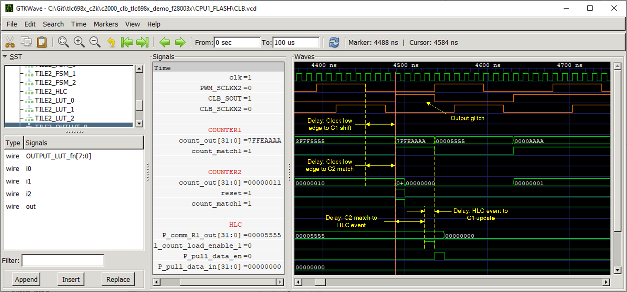 Figure 4-19 Output Glitch
The glitch can be elimited by latching the serializer output before passing to CLB_SOUT. However, this approach is not used since at least two CLB cycles of setup time are expected per the transmit simulation which is enough to meet the 10ns setup time required by the LP5891-Q1 device.