SPRAD62 February 2023 F29H850TU , F29H859TU-Q1 , TMS320F280023C , TMS320F280025C , TMS320F280025C-Q1 , TMS320F280037C , TMS320F280037C-Q1 , TMS320F280038C-Q1 , TMS320F280039C , TMS320F280039C-Q1 , TMS320F28386D , TMS320F28386D-Q1 , TMS320F28386S , TMS320F28386S-Q1 , TMS320F28388D , TMS320F28388S , TMS320F28P650DH , TMS320F28P650DK , TMS320F28P650SH , TMS320F28P650SK , TMS320F28P659DH-Q1 , TMS320F28P659DK-Q1 , TMS320F28P659SH-Q1
- Abstract
- Trademarks
- 1Introduction
- 2Serial Port Design Methodology
- 3Example A: Using the CLB to Input and Output a TDM Stream in Audio Applications
- 4Example B: Using the CLB to Implement a Custom Communication Bus for LED Driver in Lighting Applications
- 5References
2.3.1 Synchronizing Outputs Signals
In all likelihood, the output signals generated by the CLB is generated by different logic blocks in the CLB tile. This can lead to different delay paths in each output signal. In order to maximize the setup and hold times seen by the receiving device, the different CLB outputs can be synchronized to each other using a bus clock and simple flip-flops, see Figure 2-1. The flip-flops can be implemented using finite state machine (FSM) blocks in the CLB tile. However, due to limited CLB tile resources, it is best to use this option only when absolutely needed.
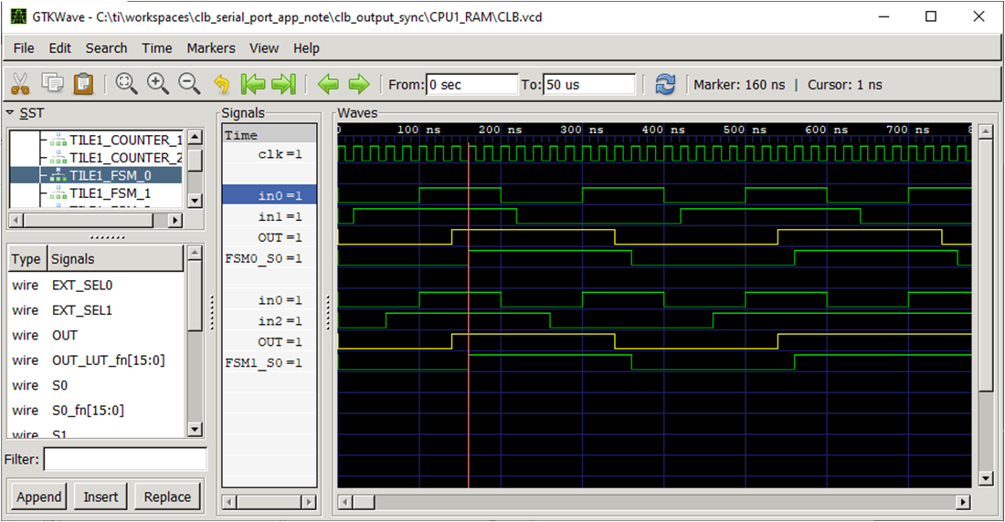
As an example of the need for synchronization logic, consider the simulation in Figure 2-2, which shows two inputs, in1 and in2, changing state at slightly different times. These two signals are synchronized to each other using a third “clock” signal, in0 using two edge-triggered D-type flip-flops implemented using the two FSMs. As can be seen from the simulation, each FSM latches and delays its input signal using the “clock” signal in0. As a result, both FSM outputs are synchronized with each other.
 Figure 2-2 Synchronizing Outputs Using
FSM D-Type Flip-FLops
Figure 2-2 Synchronizing Outputs Using
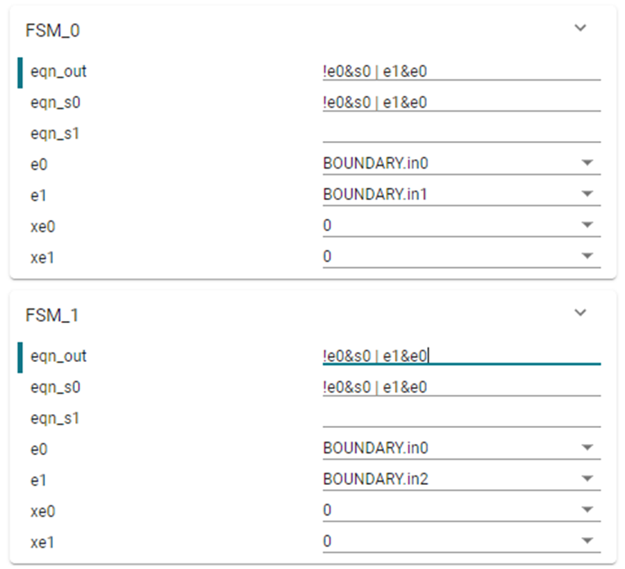
FSM D-Type Flip-FLopsThe logic equations for each FSM output and state variable are shown in Figure 2-3. Notice that both FSM out and s0 are set to the same equation and either signal can be used to drive the final output. There is a 1-cycle delay between both signals due to out being a purely combinatorial output, while s0 is always updated on the next CLB clock cycle. Also note that in this simulation, in0 input filter is setup for synchronous, rising-edge detect.
 Figure 2-3 FSM Setup for D-Type
Flip-Flop