SPRAD62 February 2023 F29H850TU , F29H859TU-Q1 , TMS320F280023C , TMS320F280025C , TMS320F280025C-Q1 , TMS320F280037C , TMS320F280037C-Q1 , TMS320F280038C-Q1 , TMS320F280039C , TMS320F280039C-Q1 , TMS320F28386D , TMS320F28386D-Q1 , TMS320F28386S , TMS320F28386S-Q1 , TMS320F28388D , TMS320F28388S , TMS320F28P650DH , TMS320F28P650DK , TMS320F28P650SH , TMS320F28P650SK , TMS320F28P659DH-Q1 , TMS320F28P659DK-Q1 , TMS320F28P659SH-Q1
- Abstract
- Trademarks
- 1Introduction
- 2Serial Port Design Methodology
- 3Example A: Using the CLB to Input and Output a TDM Stream in Audio Applications
- 4Example B: Using the CLB to Implement a Custom Communication Bus for LED Driver in Lighting Applications
- 5References
4.7.2 Software Setup
The following software packages are required to build and run the software:
- Code Composer Studio (CCS) version 11.1.0 or later
- C2000ware
version 4.02.00.00 or later
(optional) GNU compiler (TDM-GCC) and GTK Wave simulation viewer for running simulations. For more information, see the CLB Tool’s User's Guide.
Setup the LED example software by following these steps in CCS:
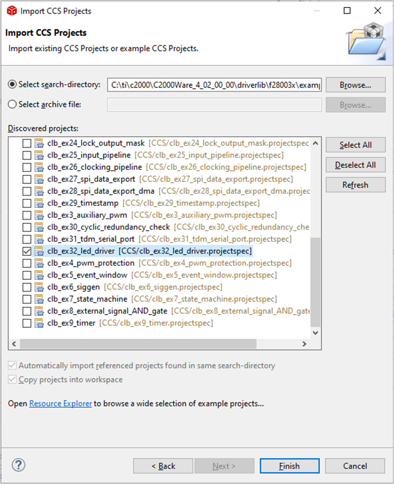
- In the CCS menu, click 'Project -> Import CCS Projects...'.
- Enter the path to the F28003x
driverlib CLB example projects in the ‘Select search-directory’.
- Path: <C2000WARE_INSTALL>\driverlib\f28003x\examples\clb
- Click ‘Refresh’.
- Select the
‘clb_ex32_led_driver’ project.
 Figure 4-20 Importing CLB LED
Driver Example Project
 - Check ‘Copy projects into workspace’.
- Click 'Finish' to complete
importing the project into the workspace.
Optional: Click 'Project -> Build Configurations -> Set Active -> CPU1_LAUNCHXL_FLASH' to build the code for flash execution.
- In the CCS menu, click 'Project -> Build Project' to build the example project.
- Right-click the TMS320F280039C_LaunchPad.ccxml file in the project and select "Set as Active Target Configuration".
- Click 'Run -> Debug' to load the executable to the F280039C target device.
- Lastly, click 'Run -> Resume' in the CCS Debug perspective to run the code.