SPRAD62 February   2023 TMS320F280023C , TMS320F280025C , TMS320F280025C-Q1 , TMS320F280037C , TMS320F280037C-Q1 , TMS320F280038C-Q1 , TMS320F280039C , TMS320F280039C-Q1 , TMS320F28386D , TMS320F28386D-Q1 , TMS320F28386S , TMS320F28386S-Q1 , TMS320F28388D , TMS320F28388S , TMS320F28P650DH , TMS320F28P650DK , TMS320F28P650SH , TMS320F28P650SK , TMS320F28P659DH-Q1 , TMS320F28P659DK-Q1 , TMS320F28P659SH-Q1


  1.   Abstract
  2.   Trademarks
  3. 1Introduction
  4. 2Serial Port Design Methodology
    1. 2.1 Step 1: Understand Design Requirements
    2. 2.2 Step 2: Identify Required Inputs to the CLB Tile
      1. 2.2.1 GPIO Input Qualification
      2. 2.2.2 CLB Input Settings
    3. 2.3 Step 3: Identify Required Outputs from CLB Logic
      1. 2.3.1 Synchronizing Outputs Signals
      2. 2.3.2 Output Signal Conditioning
    4. 2.4 Step 4: Design the CLB Logic
      1. 2.4.1 Resource Allocation
      2. 2.4.2 Exchanging Data Between CLB FIFOs and MCU RAM
      3. 2.4.3 CLB Logic Status and Trigger Flags
        1. 2.4.3.1 Status/Flag Bits
        2. 2.4.3.2 Trigger Bits
    5. 2.5 Step 5: Simulate the Logic Design
    6. 2.6 Step 6: Test the CLB Logic
  5. 3Example A: Using the CLB to Input and Output a TDM Stream in Audio Applications
    1. 3.1 Example Overview
    2. 3.2 Step 1: Understand Design Requirements
    3. 3.3 Step 2: Identify Required Inputs to the CLB Tile
    4. 3.4 Step 3: Identify Required Outputs from CLB Logic
    5. 3.5 Step 4: Design the CLB Logic
      1. 3.5.1 Resource Allocation
      2. 3.5.2 TDM Word Counter
      3. 3.5.3 FSYNC and DATA1 Output Synchronization
    6. 3.6 Step 5: Simulate the Logic Design
    7. 3.7 Step 6: Test the CLB Logic
      1. 3.7.1 Hardware Setup and Connections
      2. 3.7.2 Software Setup
      3. 3.7.3 Testing Output Setup and Hold Times
      4. 3.7.4 Testing Data Integrity
  6. 4Example B: Using the CLB to Implement a Custom Communication Bus for LED Driver in Lighting Applications
    1. 4.1 Example Overview
    2. 4.2 Step 1: Understand Design Requirements
    3. 4.3 Step 2: Identify Required Inputs to the CLB Tile
    4. 4.4 Step 3: Identify Required Outputs From CLB Logic
    5. 4.5 Step 4: Design the CLB Logic
      1. 4.5.1 TX Tile Logic
      2. 4.5.2 RX Tile Logic
      3. 4.5.3 Data Clocking
    6. 4.6 Step 5: Simulate the Logic Design
    7. 4.7 Step 6: Test the CLB Logic
      1. 4.7.1 Hardware Setup and Connections
      2. 4.7.2 Software Setup
      3. 4.7.3 Testing Output Setup and Hold Times
  7. 5References

Testing Output Setup and Hold Times

A key consideration in the output CCSI bus from the CLB is the expected setup and hold time seen by the receiving device. To measure the setup and hold time, an oscilloscope was used to continuously capture the output of the CLB.

As shown in Figure 4-21, the CLB output has a minimum setup time of approximately 55 ns which is more than enough to meet the 10 ns setup time required by the LP5891-Q1 LED driver. Note the variation in the CLB_SOUT_1 output. As described in Section 4.6, this is due to the varying internal delays in updating the serializer output. The glitch can be eliminated by latching the serializer output before passing to CLB_SOUT. However, this method is not used given that the final output has enough setup time to meet the LP5891-Q1 LED driver requirements.

The hold time is at least half of an SCLK cycle.
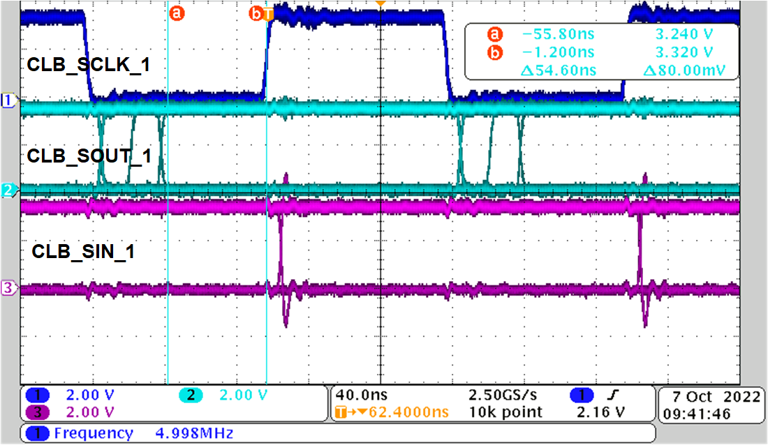
GUID-20221017-SS0I-VH8X-BGSW-392NJFJDXQ2V-low.png Figure 4-21 LED Driver Example Setup and Hold Time