SPRADC3 june 2023 AM2431 , AM2432 , AM2434 , AM2631 , AM2631-Q1 , AM2632 , AM2632-Q1 , AM2634 , AM2634-Q1 , AM263P2 , AM263P2-Q1 , AM263P4 , AM263P4-Q1 , AM3351 , AM3352 , AM3354 , AM3356 , AM3357 , AM3358 , AM3358-EP , AM3359 , AM4372 , AM4376 , AM4377 , AM4378 , AM4379 , AM5706 , AM5708 , AM5716 , AM5718 , AM5718-HIREL , AM5726 , AM5728 , AM5729 , AM5746 , AM5748 , AM5749 , AM6411 , AM6412 , AM6421 , AM6422 , AM6441 , AM6442 , AM6526 , AM6528 , AM6546 , AM6548
4 Verification
Section 2.3 and Section 2.4 show how the data transmitting accuracy and LVDS interface latency is verified. This section shows how to test the jitter on the PRU GPIO side and the processing time for both transmitting and receiving. Figure 4-1 shows the transmitting data rate with 125 MHz. Figure 4-2 and Figure 4-3 shows that the jitter on the GPO side during rising and falling edge is only 60ps.
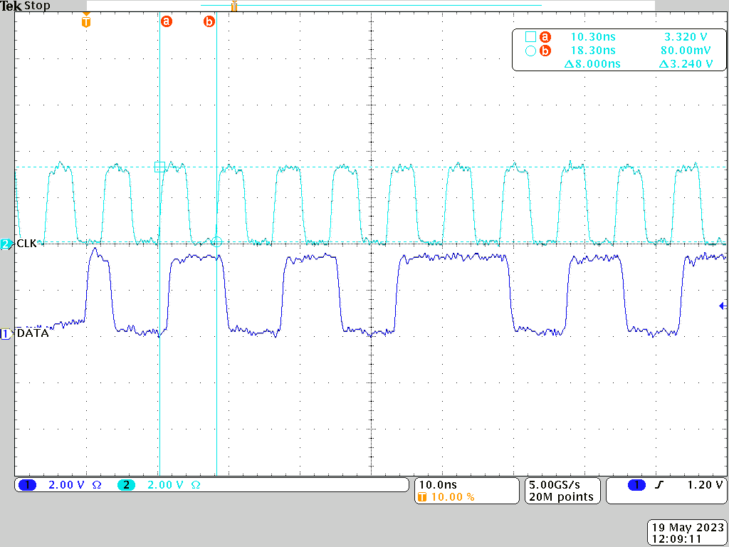 Figure 4-1 Transmitting Data Rates
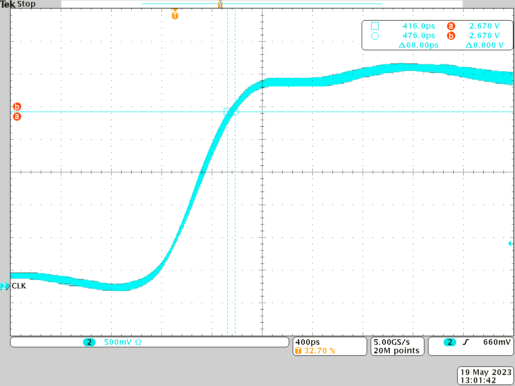 Figure 4-2 PRU GPO Jitter on Rising Edge
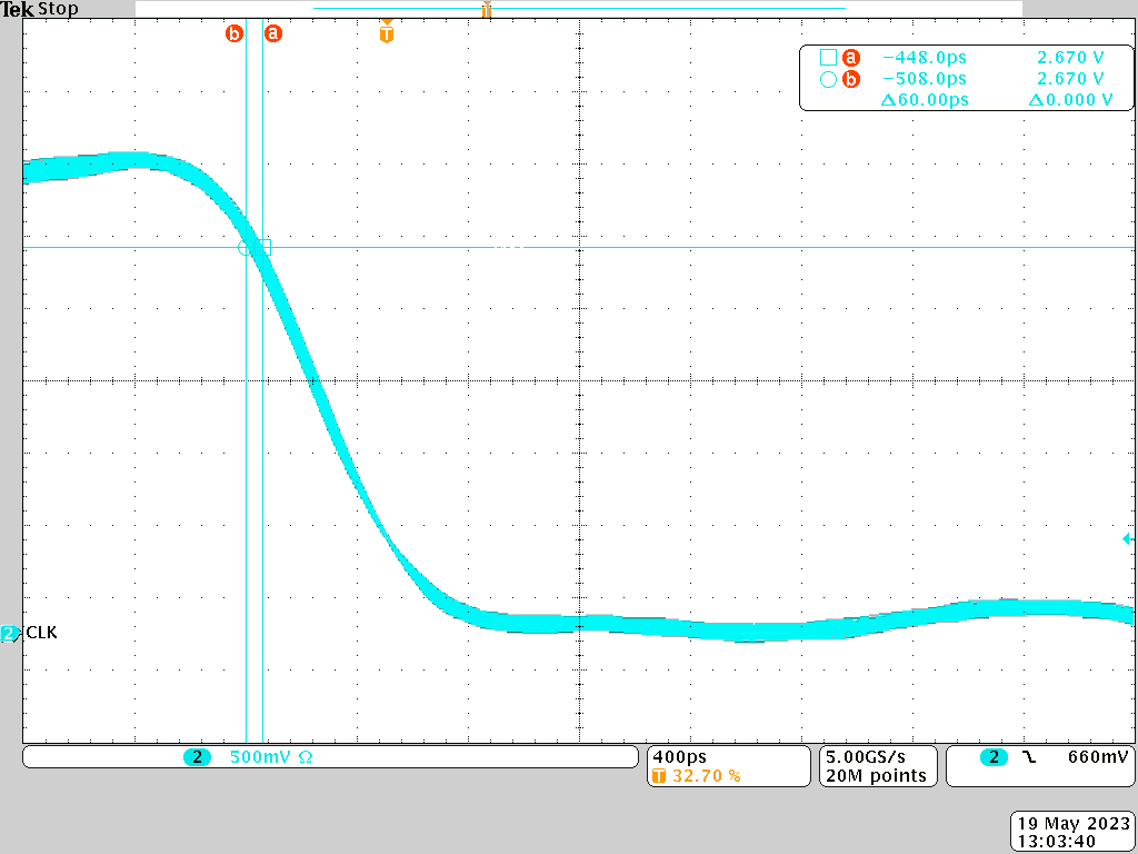 Figure 4-3 PRU GPO Jitter on Falling Edge
The processing time of transmitting data includes encode data, data CRC16 check, and IPC scratch pad memory sharing (as an option). The processing time takes 48ns for encoding 8-bit data and 20ns for a 32-bit CRC16 check under a maximum of 250 MHz PRU core clock. A 64-bit width transmitting cycle pattern requires 404ns with 384ns encoding time and 20ns CRC time. The processing time for receiving includes decode data, data CRC16 check, and IPC scratch pad memory sharing (as an option). Processing takes 60ns for decoding 10-bits of data and 20ns for a 32-bit CRC16 check under a maximum of 250 MHz PRU core clock. A 64-bit width receiving cycle pattern requires 500ns with 480ns encoding time and 20ns CRC time. Figure 4-4 through Figure 4-6 shows the test results of processing time using PRU_GPO toggling. Since the PRU_GPIO can only be configured for one mode at a time, the test condition is separated from the communication period and just tests the time for relative code instruction.
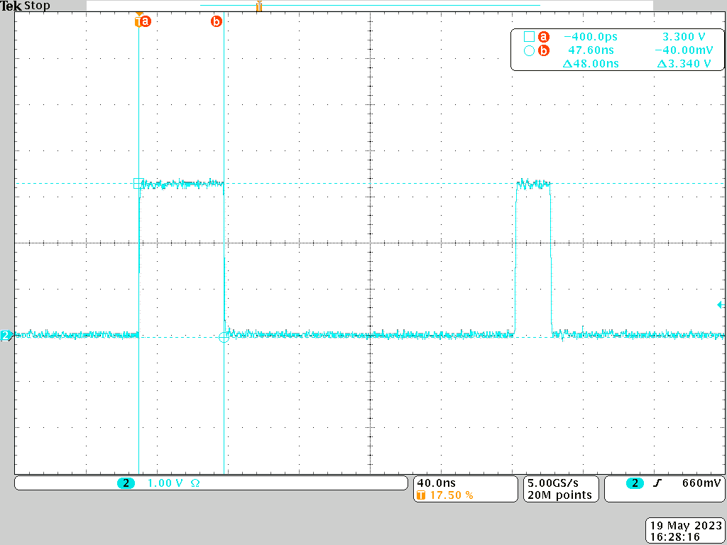 Figure 4-4 Processing Time for 8-bit Data
Encoding
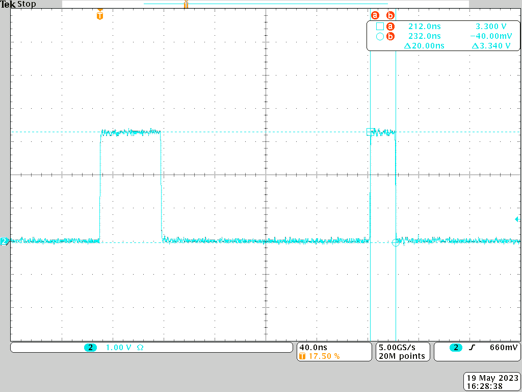 Figure 4-5 Processing Time for CRC16
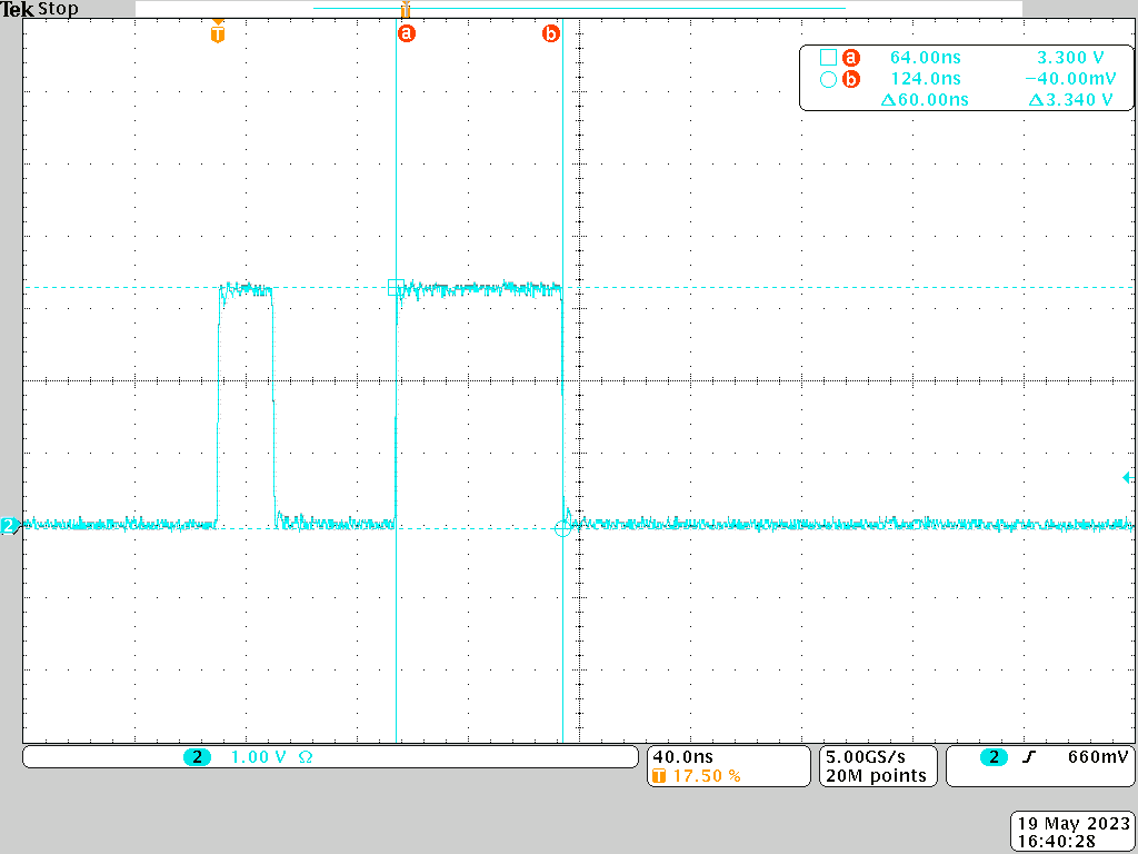 Figure 4-6 Processing Time for 10-bit Data
Decoding
Figure 4-6 Processing Time for 10-bit Data
DecodingWith the support from RTU_PRU0 and RTU_PRU1 auxiliary cores, data transfer and processing can be implemented in parallel. The IPC module can be utilized to exchange data between PRU and RTU with XFR instructions. The scratch pad (register R2:R9) is 32 bytes wide, connecting PRU and RTU_PRU cores together within a slice. XFR instructions define the start, size, direction of the operation, and device ID. Figure 4-7 shows the integration of the PRU and IPC Scratch Pad.
 Figure 4-7 Integration of the PRU and IPC Scratch
Pad
Figure 4-7 Integration of the PRU and IPC Scratch
PadThe XFR2VBUS hardware accelerator can support data movement to and from the Magneto-resistive random-access memory (MRAM) or Tightly Coupled random-access Memory (TCRAM). Both XFR2VBUS TX and RX buffers are 64-bytes deep and can transfer 64 bytes of data with a single register transfer in (XIN) or register transfer out (XOUT) instruction. The following code example shows the data movement to and from TCRAM using the XFR2VBUS widget.
; Read wait
wait_till_read_busy_0?:
  xin XFR2VBUSP_RD0_XID, &r18, 1
  qbbs wait_till_read_busy_0?, r18, 3    ; R18.3 :RD_MST_REQ Wait until Last Data has been latched

; TCM to XFR2VBUS RX buffer
  ldi   r18, 6                           ; 64 bytes
  ldi32 r19, CSL_R5FSS0_CORE0_ATCM_BASE  ; TCM Address
  ldi   r20, 0
  xout  XFR2VBUSP_RD0_XID, &r18, 10      ; transfer address
  xin   XFR2VBUSP_RD0_XID, &r2, 65       ; transfer data

; Write wait
wait_till_write_done_0?:
  xin   XFR2VBUSP_WR0_XID, &r20, 1
  qbbs  wait_till_write_done_0?, r20, 0  ; R20.0 : WR_BUSY Wait until Idle

; XFR2VBUS TX buffer to TCM
  ldi32 r18, CSL_R5FSS0_CORE0_ATCM_BASE  ; TCM Address
  ldi   r19, 0
  xout  XFR2VBUSP_RD0_XID, &r18, 10      ; transfer address
  xin   XFR2VBUSP_RD0_XID, &r2, 65       ; transfer data
PRUn can start transmitting data after the first 16-bit raw data is encoded by RTU_PRUn. Similarly, RTU_PRUn in the receiving path can start decoding data after the first 20-bit encoded data is received by PRUn. The transmitting processing time of 64-bit width cycle patterns can be reduced from 404ns to 96ns (16-bit data encoding) and the receiving processing time of 64-bit width cycle patterns can be reduced from 500ns to 120ns (20-bit data decoding). Table 4-1 summarizes the processing times with and without the support of the RTU_PRUn cores.
| PRU cores | Sampling
clock (MHz) |
Data
length (bit) |
TX module
data processing time (ns) |
Data
transfer time (ns) |
RX module
data processing time (ns) |
Total
time (ns) |
|---|---|---|---|---|---|---|
| PRU | 125 | 64 | 404 | 640(1) | 500 | 1544 |
| PRU + RTU | 125 | 64 | 96 | 640(1) | 120 | 856 |
80-bit encoded data width for data transfer