SPRADC3 june 2023 AM2431 , AM2432 , AM2434 , AM2631 , AM2631-Q1 , AM2632 , AM2632-Q1 , AM2634 , AM2634-Q1 , AM263P2 , AM263P2-Q1 , AM263P4 , AM263P4-Q1 , AM3351 , AM3352 , AM3354 , AM3356 , AM3357 , AM3358 , AM3358-EP , AM3359 , AM4372 , AM4376 , AM4377 , AM4378 , AM4379 , AM5706 , AM5708 , AM5716 , AM5718 , AM5718-HIREL , AM5726 , AM5728 , AM5729 , AM5746 , AM5748 , AM5749 , AM6411 , AM6412 , AM6421 , AM6422 , AM6441 , AM6442 , AM6526 , AM6528 , AM6546 , AM6548
2.5 LVDS and M-LVDS Interface
Low-voltage Differential Signaling (LVDS) devices generally comply with the American National Standards Institute (ANSI) standard TIA/EIA-644. And the Multipoint Low Voltage Differential Signaling (M-LVDS) comply with ANSI TIA/EIA-899. Table 2-1 highlights some of the important specifications for drivers and receivers between LVDS and M-LVDS.
| Parameter | TIA/EIA-644-A (LVDS REV A) | TIA/EIA-899 (M-LVDS) | Unit |
|---|---|---|---|
| Driver characteristics | |||
| Offset voltage: Vos (maximum) | 1375 | 2100 | mV |
| Offset voltage: Vos (minimum) | 1125 | 300 | mV |
|
Differential output voltage: Vod (maximum) |
454 (100 Ω) | 650 (50 Ω) | mV |
| Differential output voltage: Vod (minimum) | 247 (100 Ω) | 480 (50 Ω) | mV |
| Offset voltage variation: Vospp | 150 | 150 | mV |
| Short circuit current: Ios | 12/24 | 43 | mA |
| Differential voltage change: ΔVod | 50 | 50 | mV |
| Offset voltage change: ΔVos | 50 | 50 | mV |
| Transition time: tr/tf (minimum) | 260 | 1000 | ps |
| Receiver characteristics | |||
| Ground potential difference: Vgpd | ±1 | ±1 | V |
| Input leakage current: Iin | 20 | 20 | μA |
| Differential input leakage current: Iid | 6 | 4 | μA |
| Input voltage range: Vin | 0 to 2.4 | -1.4 to 3.8 | V |
| Input threshold: Vith | 100 | 50 | mV |
Intra drive communication designs require high speed, low power and electromagnetic compatibility. Hence, LVDS devices provide a wide range of solutions for intra drive communication designs from point-to-point to multidrop data transmission. The data transfer rate can range from up to 1500Mbps with a 100-meter cable length and only required 1.2 mW power consumption. Differential signals also help by having high noise immunity. The DS90x series for LVDS and SN65MLVDSx series for M-LVDS from Texas Instruments incorporates a wide variety of single and multichannel devices for designers. Moreover, TI’s ISO7821LLx series provides reinforced isolation with LVDS interface when required in intra drive designs, especially for cold-hot side control applications. The intra drive communication block diagram with LVDS interface and PRU is shown as Figure 2-10.
 Figure 2-10 Intra Drive Communication Block
Diagram With LVDS Interface and PRU
Figure 2-10 Intra Drive Communication Block
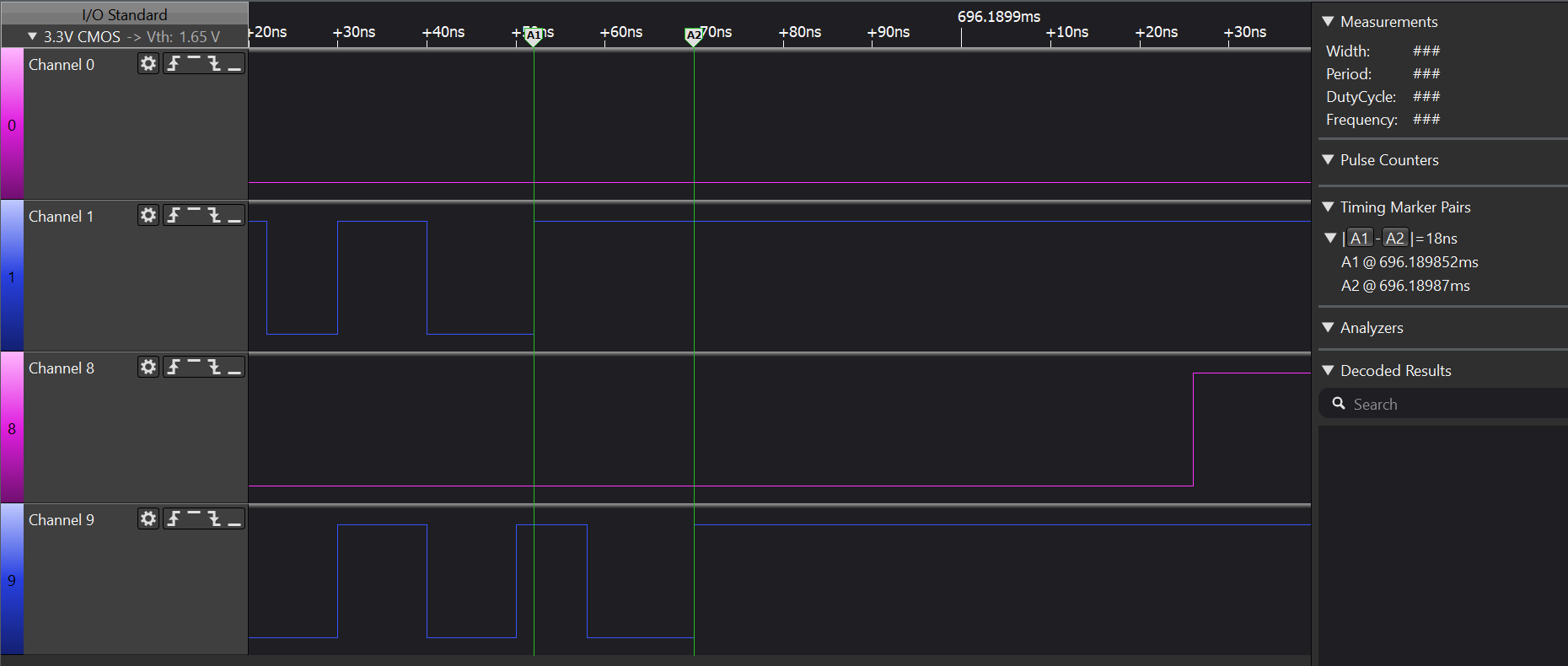
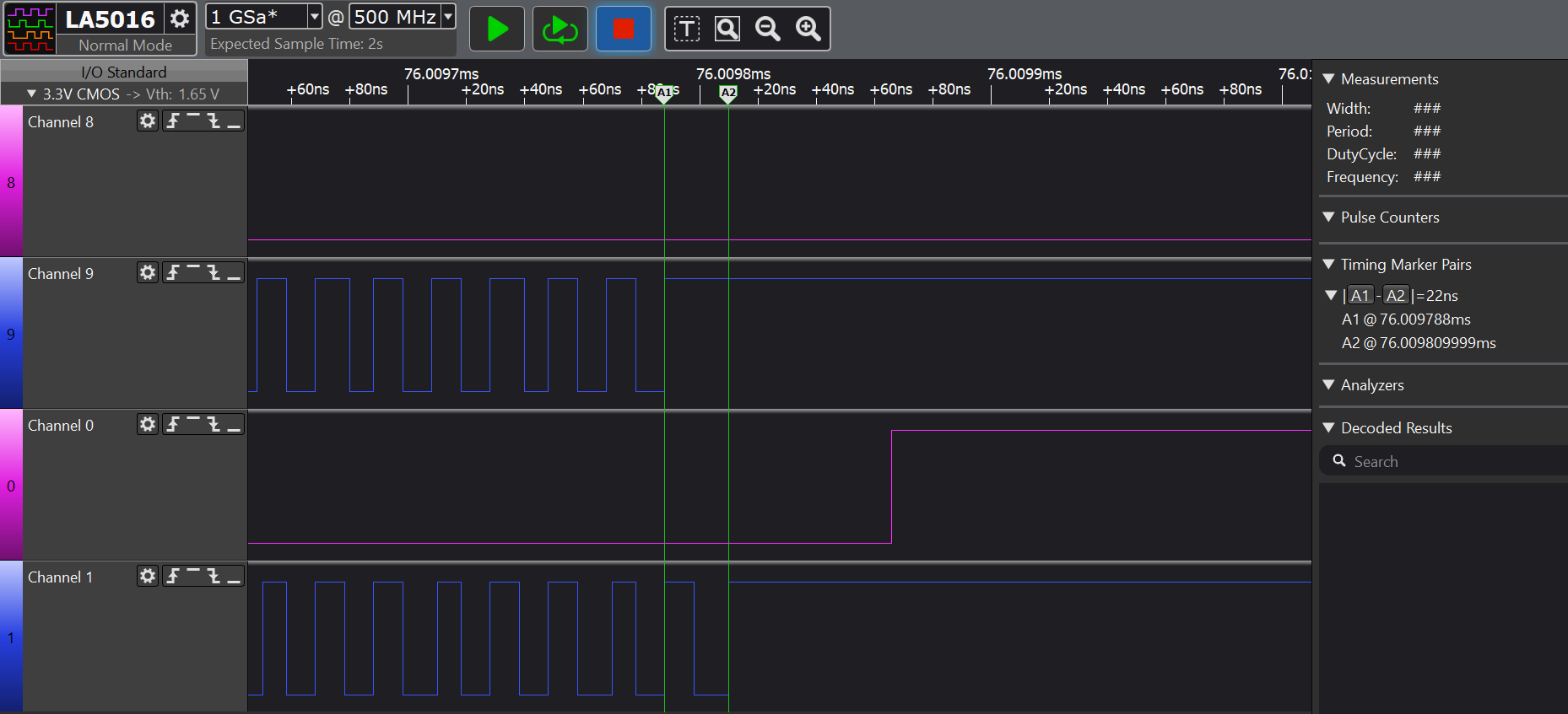
Diagram With LVDS Interface and PRUTo verify the latency of LVDS transceivers and isolators, a 100 MHz clock signal is sent by PRU_GPO using the DS90LV049+ISO7821LL for LVDS interface and SM65MLVDS203+ISO7840 for M-LVDS interface. Figure 2-11 and Figure 2-12 show the latency for LVDS interface is 18ns and for M-LVDS interface is 22ns.
 Figure 2-11 18ns Latency for DS90LV049 and
ISO7821LL LVDS Interfaces
 Figure 2-12 22ns Latency for SN65MLLVDS203 and
ISO7840 M-LVDS Interfaces