SPRUIY9B May 2021 – October 2023
- 1
- Abstract
- Trademarks
- 1Key Features
- 2EVM Revisions and Assembly Variants
- 3Important Usage Notes
-
4System Description
- 4.1 Key Features
- 4.2 Functional Block Diagram
- 4.3 Power-On/Off Procedures
- 4.4
Peripheral and Major Component
Description
- 4.4.1 Clocking
- 4.4.2 Reset
- 4.4.3 Power
- 4.4.4 Configuration
- 4.4.5 JTAG
- 4.4.6 Test Automation
- 4.4.7 UART Interface
- 4.4.8 Memory Interfaces
- 4.4.9 Ethernet Interface
- 4.4.10 USB 3.0 Interface
- 4.4.11 PRU Connector
- 4.4.12 User Expansion Connector
- 4.4.13 MCU Connector
- 4.4.14 Interrupt
- 4.4.15 I2C Interface
- 4.4.16 IO Expander (GPIOs)
-
5Known Issues
- 5.1 Issue 1: LP8733x Max output Capacitance Spec Exceeded on LDO0 and LDO1
- 5.2 Issue 2: LP8733x Output Voltage of 0.9V Exceeds AM64x VDDR_CORE max Voltage Spec of 0.895 V
- 5.3 Issue 3 - SDIO Devices on MMC0 Require Careful Trace Lengths to Meet Interface Timing Requirements
- 5.4 Issue 4 - LPDDR4 Data Rate Limitation in Stressful Conditions
- 5.5 Issue 5 - Junk Character
- 5.6 Issue 6 - Test Power Down Signal Floating
- 5.7 Issue 7 - uSD Boot Not Working
- 6Regulatory Compliance
- 7Revision History
4.4.8.1 LPDDR4 Interface
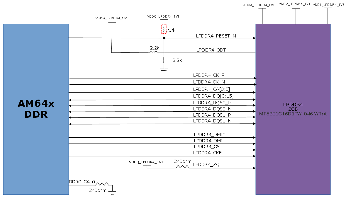
The SK EVM has 2GB, 16bit wide LPDDR4 memory with operating data rate of 4226Mbps per pin. Micron's MT53E1G16D1FW-046 WT: A is used. The LPDDR memory is mounted on-board (single chip) and requires 1.1V and thus reduces power demand. The LPDDR4 device requires I/O power and core 2 power of 1.1V, DRAM activating power supply (core 1) of 1.8V.
LPDDR4 reset is active low signal, which is controlled by SOC and the signal is pulled up to set the default active state and a footprint for pull-down is also provided. A 240 Ω resistor is connected from ZQ pin to 1.1V supply for LPDDR4 device and SoC DDR0_CAL pin is grounded.
The ODT (On Die Termination) is applied to DQ, DQS and DM_n signals. The device is capable of providing three different ODT modes: Nominal, Dynamic and Park with termination values: RTT (Park), RTT (NOM), and RTT (WR). Figure 4-14 shows the DDR interface between LPDDR4 and AM64x.
 Figure 4-14 LPDDR4 Interface