SPRUIY9B May 2021 – October 2023
- 1
- Abstract
- Trademarks
- 1Key Features
- 2EVM Revisions and Assembly Variants
- 3Important Usage Notes
-
4System Description
- 4.1 Key Features
- 4.2 Functional Block Diagram
- 4.3 Power-On/Off Procedures
- 4.4
Peripheral and Major Component
Description
- 4.4.1 Clocking
- 4.4.2 Reset
- 4.4.3 Power
- 4.4.4 Configuration
- 4.4.5 JTAG
- 4.4.6 Test Automation
- 4.4.7 UART Interface
- 4.4.8 Memory Interfaces
- 4.4.9 Ethernet Interface
- 4.4.10 USB 3.0 Interface
- 4.4.11 PRU Connector
- 4.4.12 User Expansion Connector
- 4.4.13 MCU Connector
- 4.4.14 Interrupt
- 4.4.15 I2C Interface
- 4.4.16 IO Expander (GPIOs)
-
5Known Issues
- 5.1 Issue 1: LP8733x Max output Capacitance Spec Exceeded on LDO0 and LDO1
- 5.2 Issue 2: LP8733x Output Voltage of 0.9V Exceeds AM64x VDDR_CORE max Voltage Spec of 0.895 V
- 5.3 Issue 3 - SDIO Devices on MMC0 Require Careful Trace Lengths to Meet Interface Timing Requirements
- 5.4 Issue 4 - LPDDR4 Data Rate Limitation in Stressful Conditions
- 5.5 Issue 5 - Junk Character
- 5.6 Issue 6 - Test Power Down Signal Floating
- 5.7 Issue 7 - uSD Boot Not Working
- 6Regulatory Compliance
- 7Revision History
4.4.5 JTAG
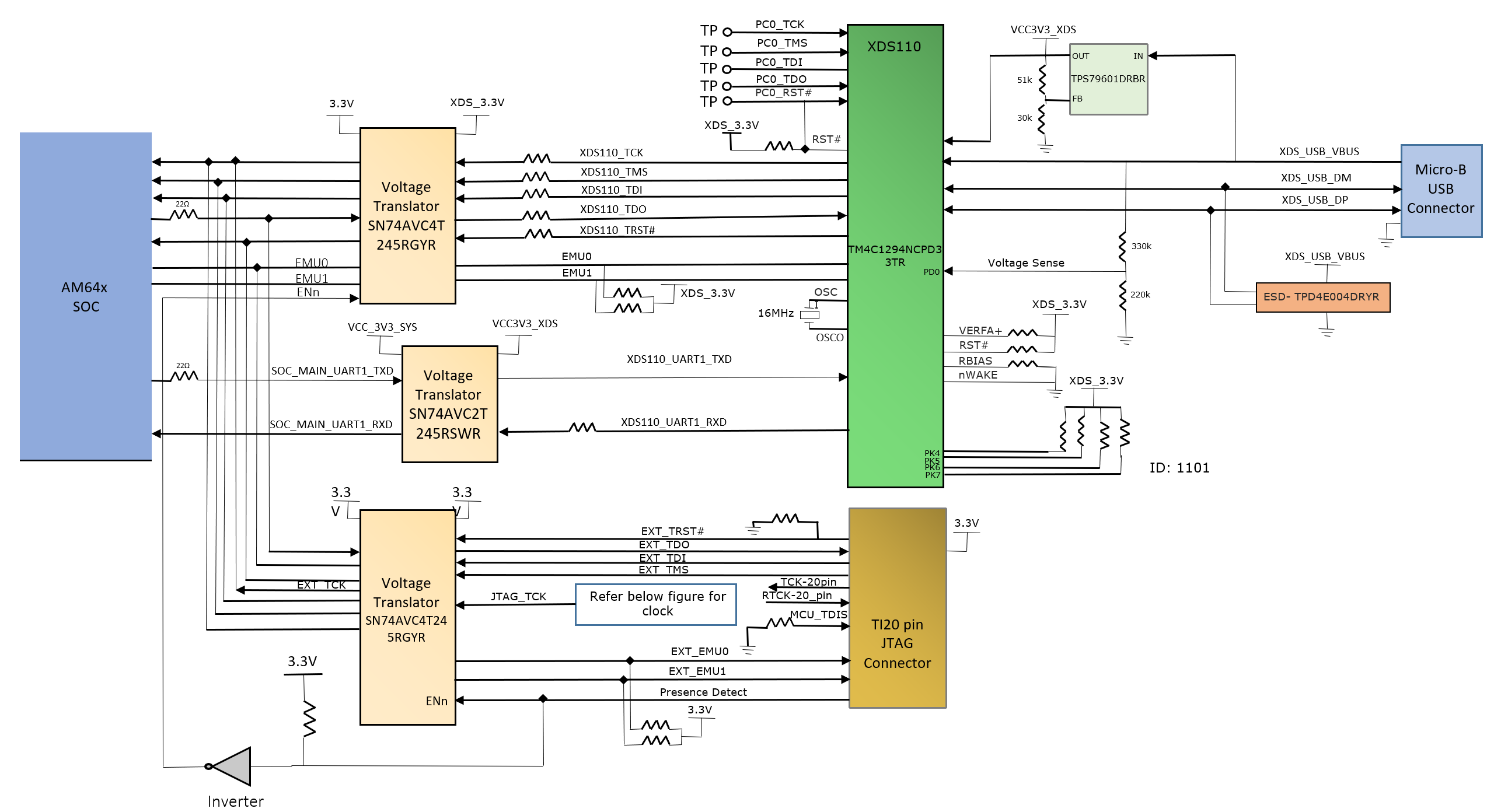
Optionally, a JTAG Interface on SKEVM is also provided through a 20 Pin Standard JTAG cTI Header (J14). This allows the user to connect an external JTAG Emulator. Voltage translation buffers are used to isolate the JTAG signals from the cTI header from the rest of the EVM. The output from the voltage translators from the XDS110 Section and cTI Header Section is muxed and connected to the SoC JTAG Interface. If a connection to the cTI 20 Pin JTAG connector is sensed using a present detect circuit, then the mux are set to route the 20pin signals to the AM64x in place of the on-board emulation circuit.
The pin-outs of cTI 20 pin JTAG connector J14 are given in Table 4-13. An ESD protection (part number TPD4E004) is provided on the USB signals to steer ESD current pulses to VCC or GND. TPD4E004 protects against ESD pulses up to ±15-kV Human-Body Model (HBM) as specified in IEC 61000-4-2 and provides ±8-kV contact discharge and ±12- kV air-gap discharge. For cTI 20 pin connector pin-out details, see Table 4-13.
| Pin No. | Signal | Pin No. | Signal |
|---|---|---|---|
| 1 | JTAG_TMS | 11 | JTAG_cTI_TCK |
| 2 | JTAG_TRST# | 12 | DGND |
| 3 | JTAG_TDI | 13 | JTAG_EMU0 |
| 4 | JTAG_TDIS | 14 | JTAG_EMU1 |
| 5 | VCC_3V3_SYS | 15 | JTAG_EMU_RSTN |
| 6 | NC | 16 | DGND |
| 7 | JTAG_TDO | 17 | NC |
| 8 | SEL_XDS110_INV | 18 | NC |
| 9 | JTAG_cTI_RTCK | 19 | NC |
| 10 | DGND | 20 | DGND |
 Figure 4-11 JTAG Interface
The SKEVM board includes XDS110-class on board emulation and a test automation header to support TI internal testing of software builds. The connection for the emulator uses an USB2.0 micro-B connector (J12) and the circuit acts as a powered USB slave device. The VBUS power from the connector is used to power the emulation circuit such that connection to the emulator is not lost when the power to the EVM is removed. Voltage translation buffers are used to isolate the XDS110 circuit from the rest of the EVM. Additionally, XDS110 also offers UART to USB signal translation on the same USB port. UART1 of the SoC MAIN Domain without flow control is connected to the XDS110 UART port via an isolator.