SPRUIY9B May 2021 – October 2023
- 1
- Abstract
- Trademarks
- 1Key Features
- 2EVM Revisions and Assembly Variants
- 3Important Usage Notes
-
4System Description
- 4.1 Key Features
- 4.2 Functional Block Diagram
- 4.3 Power-On/Off Procedures
- 4.4
Peripheral and Major Component
Description
- 4.4.1 Clocking
- 4.4.2 Reset
- 4.4.3 Power
- 4.4.4 Configuration
- 4.4.5 JTAG
- 4.4.6 Test Automation
- 4.4.7 UART Interface
- 4.4.8 Memory Interfaces
- 4.4.9 Ethernet Interface
- 4.4.10 USB 3.0 Interface
- 4.4.11 PRU Connector
- 4.4.12 User Expansion Connector
- 4.4.13 MCU Connector
- 4.4.14 Interrupt
- 4.4.15 I2C Interface
- 4.4.16 IO Expander (GPIOs)
-
5Known Issues
- 5.1 Issue 1: LP8733x Max output Capacitance Spec Exceeded on LDO0 and LDO1
- 5.2 Issue 2: LP8733x Output Voltage of 0.9V Exceeds AM64x VDDR_CORE max Voltage Spec of 0.895 V
- 5.3 Issue 3 - SDIO Devices on MMC0 Require Careful Trace Lengths to Meet Interface Timing Requirements
- 5.4 Issue 4 - LPDDR4 Data Rate Limitation in Stressful Conditions
- 5.5 Issue 5 - Junk Character
- 5.6 Issue 6 - Test Power Down Signal Floating
- 5.7 Issue 7 - uSD Boot Not Working
- 6Regulatory Compliance
- 7Revision History
4.4.8.2.2 WiLink Interface
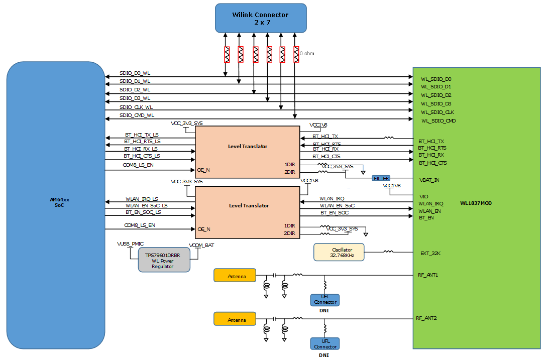
The SKEVM board has WiLink Module (WL1837MODGIMOCT) from TI connected to MMC0 port of the AM64x SoC. The WL1837MOD is a Wi-Fi, dual-band, 2.4- and 5-GHz module solution with two antennas (W3006) supporting Industrial temperature grade. The Module is connected to 4-bit IO of the MMC0 interface supporting IEEE standard 802.11a/b/g/n data rates with 20 or 40-MHz SISO or 20-MHz MIMO. The Module offers high throughput and extended range along with Wi-Fi and Bluetooth coexistence in a power-optimized design.
The device supports the following Bluetooth features:
- Bluetooth 4.2 secure connection as well as CSA2
- Concurrent operation and built-in coexisting and prioritization handling of Bluetooth and Bluetooth low energy wireless technology, audio processing, and WLAN
- Dedicated audio processor supporting on-chip SBC encoding + A2DP
- Assisted A2DP (A3DP): SBC encoding implemented internally
- Assisted WB-speech (AWBS): modified SBC codec implemented internally. Figure 4-16 shows the block diagram of Wilink module interfaced with AM64x.
SKEVM does not support A2DP BT Audio profile or HF profile.
The Module requires two power supplies, 3.3V for VBAT_IN and 1.8V for VIO_IN. WL1837MOD WiLink module is supplied from PMIC and also provided through a dedicated regulator (This is optional and DNI by default).
The MMC0 interface of SOC is powered by VDDSHV_MMC0 power supply, which is connected to 1.8V IO supply. Bluetooth UART signals, enable of BT and WLAN and WLAN_IRQ signals are connected to GPIO’s of AM64x using level translator (SN74AVC4T245RSVR). Input clock is provided by using 32.768 KHz oscillator.
Test points are provided on MMC0_DAT [4:7] pins of SOC and WL_GPIO, BT_UART_DEBUG, WL_UART_DEBUG pins on WL1837 Module.
14 pin Wi-link connector is also provided. An external Wi-Fi module (Bluetooth module is not supported) can be communicated with SoC through the 14 pin Wi-Link connector. By default, 14 pin Wi-link connector and 0E resistors are not populated on the signals which are connected to the 14 pin Wi-link connector
 Figure 4-16 WiLink Module Interface