SPRUIY9B May 2021 – October 2023
- 1
- Abstract
- Trademarks
- 1Key Features
- 2EVM Revisions and Assembly Variants
- 3Important Usage Notes
-
4System Description
- 4.1 Key Features
- 4.2 Functional Block Diagram
- 4.3 Power-On/Off Procedures
- 4.4
Peripheral and Major Component
Description
- 4.4.1 Clocking
- 4.4.2 Reset
- 4.4.3 Power
- 4.4.4 Configuration
- 4.4.5 JTAG
- 4.4.6 Test Automation
- 4.4.7 UART Interface
- 4.4.8 Memory Interfaces
- 4.4.9 Ethernet Interface
- 4.4.10 USB 3.0 Interface
- 4.4.11 PRU Connector
- 4.4.12 User Expansion Connector
- 4.4.13 MCU Connector
- 4.4.14 Interrupt
- 4.4.15 I2C Interface
- 4.4.16 IO Expander (GPIOs)
-
5Known Issues
- 5.1 Issue 1: LP8733x Max output Capacitance Spec Exceeded on LDO0 and LDO1
- 5.2 Issue 2: LP8733x Output Voltage of 0.9V Exceeds AM64x VDDR_CORE max Voltage Spec of 0.895 V
- 5.3 Issue 3 - SDIO Devices on MMC0 Require Careful Trace Lengths to Meet Interface Timing Requirements
- 5.4 Issue 4 - LPDDR4 Data Rate Limitation in Stressful Conditions
- 5.5 Issue 5 - Junk Character
- 5.6 Issue 6 - Test Power Down Signal Floating
- 5.7 Issue 7 - uSD Boot Not Working
- 6Regulatory Compliance
- 7Revision History
4.4.13 MCU Connector
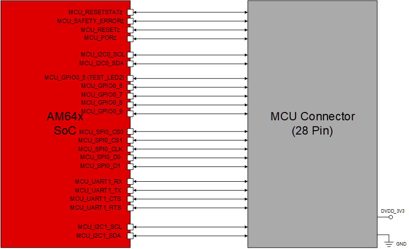
A safety signal connector is 14x2 standard 0.1” spaced header. MCU connector only includes signals connected to the MCU. 18 Signals include MCU_I2C0, MCI_I2C1, MCU_UART1 (with flow control), MCU_SPI0 and MCU_SPI1 signals. Additional control signals provided on the connector include CONN_MCU_RESETz, CONN_MCU_PORz, MCU_RESETSTATz, MCU_SAFETY_ERRORn, 3.3V IO to MCU and GND. The MCU connector does not include the Board ID memory interface. Allowed current limit is 100 mA on 3.3V rail.
Table 4-22 28 Pin MCU Connector
| Pin | Net Name | Pin | Net Name |
|---|---|---|---|
| 1 | VCC_3V3_SYS | 2 | DGND |
| 3 | MCU_SPI0_CS1 | 4 | MCU_SPI0_D1 |
| 5 | MCU_GPIO0_8 | 6 | MCU_SPI0_D0 |
| 7 | DGND | 8 | MCU_SPI0_CS0 |
| 9 | TEST_LED2 | 10 | MCU_GPIO0_6 |
| 11 | MCU_GPIO0_7 | 12 | MCU_UART1_CTS_3V3 |
| 13 | MCU_UART1_RX_3V3 | 14 | MCU_GPIO0_9 |
| 15 | DGND | 16 | MCU_I2C1_SDA |
| 17 | MCU_UART1_RTS_3V3 | 18 | MCU_SPI0_CLK |
| 19 | MCU_UART1_TX_3V3 | 20 | DGND |
| 21 | MCU_I2C0_SDA | 22 | MCU_I2C1_SCL |
| 23 | MCU_RESETSTATz | 24 | MCU_I2C0_SCL |
| 25 | CONN_MCU_RESETz | 26 | MCU_SAFETY_ERRORz_3V3 |
| 27 | DGND | 28 | CONN_MCU_PORz |
 Figure 4-26 28-Pin MCU Connector