SPRUIY9B May 2021 – October 2023
- 1
- Abstract
- Trademarks
- 1Key Features
- 2EVM Revisions and Assembly Variants
- 3Important Usage Notes
-
4System Description
- 4.1 Key Features
- 4.2 Functional Block Diagram
- 4.3 Power-On/Off Procedures
- 4.4
Peripheral and Major Component
Description
- 4.4.1 Clocking
- 4.4.2 Reset
- 4.4.3 Power
- 4.4.4 Configuration
- 4.4.5 JTAG
- 4.4.6 Test Automation
- 4.4.7 UART Interface
- 4.4.8 Memory Interfaces
- 4.4.9 Ethernet Interface
- 4.4.10 USB 3.0 Interface
- 4.4.11 PRU Connector
- 4.4.12 User Expansion Connector
- 4.4.13 MCU Connector
- 4.4.14 Interrupt
- 4.4.15 I2C Interface
- 4.4.16 IO Expander (GPIOs)
-
5Known Issues
- 5.1 Issue 1: LP8733x Max output Capacitance Spec Exceeded on LDO0 and LDO1
- 5.2 Issue 2: LP8733x Output Voltage of 0.9V Exceeds AM64x VDDR_CORE max Voltage Spec of 0.895 V
- 5.3 Issue 3 - SDIO Devices on MMC0 Require Careful Trace Lengths to Meet Interface Timing Requirements
- 5.4 Issue 4 - LPDDR4 Data Rate Limitation in Stressful Conditions
- 5.5 Issue 5 - Junk Character
- 5.6 Issue 6 - Test Power Down Signal Floating
- 5.7 Issue 7 - uSD Boot Not Working
- 6Regulatory Compliance
- 7Revision History
4.4.8.2.1 Micro SD Interface
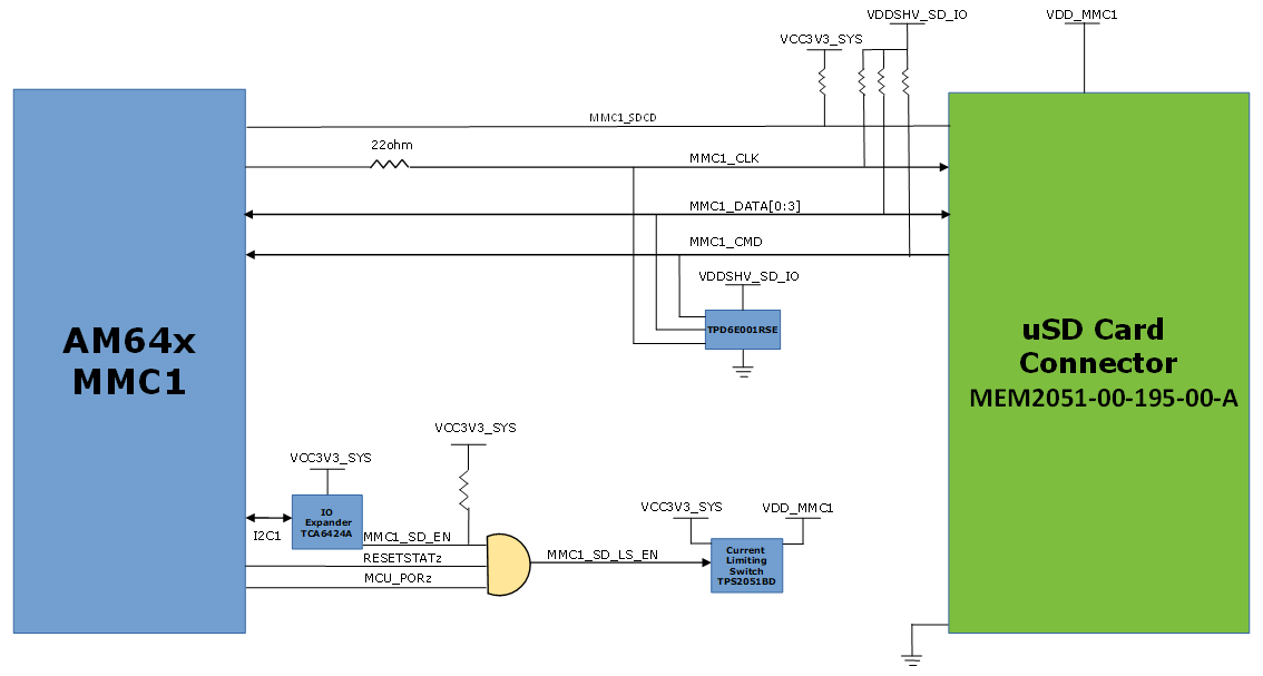
The SKEVM board provides a micro SD card interface connected to MMC1 port of AM64x SOC. The micro-SD card interface supports 16 GB density with UHS1 operation including IO operations at both 1.8V and 3.3V. The circuit included in AM64x SoC to support the IO voltage switching is connected to IO voltage of SD signals to allow the processor to negotiate IO voltage. For high-speed cards, ROM Code of SOC attempts to find the fastest speed that the card and controller can support and can have a transition to 1.8V. The internal SDIO LDO output from the SOC available at CAP_VDDSHV_SDLDO pin is connected to IO voltage of SD signals and VDDSHV_MMC1 power pins of SOC, which is the power supply for MMC1 interface.
An ESD protection device (TPD6E001RSE) is provided for data, clock and command signals. TPD6E001RSE is a line termination device with integrated TVS diodes providing system-level IEC 61000-4-2 ESD protection, ± 8-kV contact discharge and ± 15kV air-gap discharge.
The SD card is set to operate in SD mode. The CD (card detect) pin of SD card connector is pulled low and connected to CD pin of SOC. Figure 4-15 shows the block diagram of micro-SD card interface.
 Figure 4-15 Micro SD Interface