SPRUJ09D March 2022 – September 2023 AM2631 , AM2631-Q1 , AM2632 , AM2632-Q1 , AM2634 , AM2634-Q1 , AM263P2-Q1 , AM263P4 , AM263P4-Q1
- 1
- Abstract
- Trademarks
- 1Preface: Read This First
- 2Control Card Overview
- 3Board Setup
- 4Hardware Description
- 5References
- Revision History
- A E2 Design Changes
- B E1 HSEC Pinout Table
4.6.1 RGMII
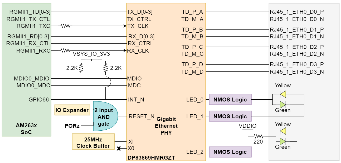
The AM263x Control Card uses one port of RGMII signals to be connected to a 48-pin ethernet PHY (DP83869HMRGZT). The PHY is configured to advertise 1-Gb operation. The ethernet data signals of the PHY are terminated to an RJ45 connector. The RJ45 connector is used on the board for Ethernet 10/100/1000 Mbps connectivity with integrated magnetic and LEDs for link and activity indication.
 Figure 4-9 RGMII1 Gigabit Ethernet
PHY
Figure 4-9 RGMII1 Gigabit Ethernet
PHYThe Ethernet PHY requires three separate power sources. VDDIO is the 3.3V, system generated supply. There are dedicated LDO's for the 1.1 V and 2.5 V supplies for the Ethernet PHY.
There are series termination resistors on the transmit and receive clock signals located near the AM263x SoC.
The MDIO and Interrupt signals from the SoC to the PHY require 2.2KΩ pull up resistors to the I/O supply voltage for proper operation. The interrupt signal is driven by a GPIO signal that is mapped from the AM263x SoC.
The reset signal for the Ethernet PHY is driven by a 2-input AND gate. The AND gate's inputs are a GPIO signal that is generated by the IO Expander and PORz.
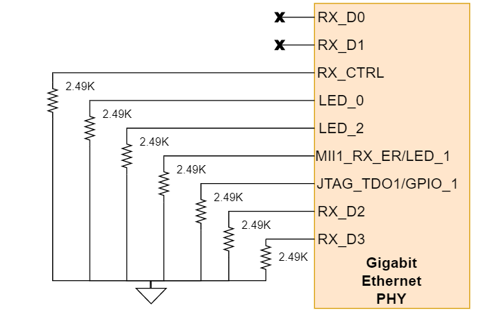
The Ethernet PHY uses many functional pins as strap option to place the device into specific modes of operation.
 Figure 4-10 RGMII1 Gigabit Ethernet PHY
Strapping Resistors
Figure 4-10 RGMII1 Gigabit Ethernet PHY
Strapping Resistors| Functional Pin | Default Mode | Mode in CC | Function |
|---|---|---|---|
| RX_D0 | 0 | 0 | PHY address: 0000 |
| RX_D1 | 0 | 0 | |
| JTAG_TDO/GPIO_1 | 0 | 0 | RGMII to Copper |
| RX_D3 | 0 | 0 | |
| RX_D2 | 0 | 0 | |
| LED_0 | 0 | 0 | Auto-negotiation, 1000/100/10 advertised, auto MDI-X |
| RX_ER | 0 | 0 | |
| LED_2 | 0 | 0 | |
| RX_DV | 0 | 0 | Port Mirroring Disabled |