TIDT244 July 2021
4.7 Bias Voltage Switch Nodes
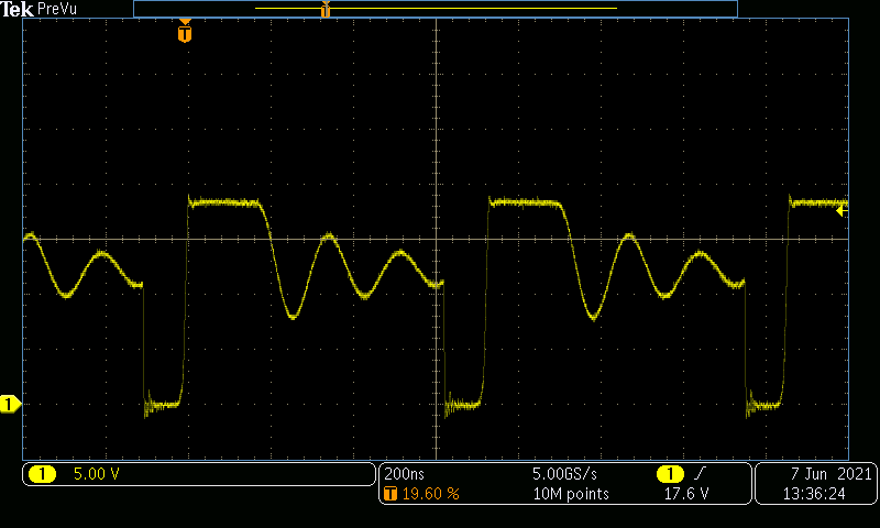
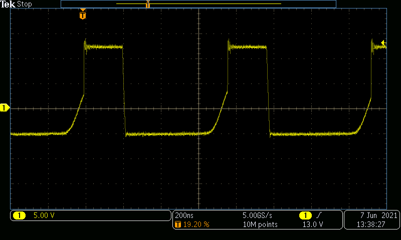
The +18-V and –5-V rails are converted from an external 12-V bias signal. The following figures show the switching behaviors of these bias converters.
 Figure 4-13 +18 V Boost Converter Switch
Node at TP9, VIN = 400 V and VOUT = 400 V at 2 A (5 V/DIV,
200 ns/DIV, BWL = 800 MHz)
 Figure 4-14 –5 V Inverting Buck-Boost
Converter Switch Node at TP17, VIN = 400 V and VOUT = 400
V at 2 A (5 V/DIV, 200 ns/DIV, BWL = 800 MHz)