TIDT244 July   2021


  1. 1Description
  2. 2Test Prerequisites
    1. 2.1 Voltage and Current Requirements
    2. 2.2 Required Equipment
  3. 3Testing and Results
    1. 3.1 Thermal Images
    2. 3.2 Efficiency and Power Dissipation Graph
    3. 3.3 Efficiency and Power Dissipation Data
    4. 3.4 Current Regulation
    5. 3.5 Voltage Regulation
  4. 4Waveforms
    1. 4.1 Start-up
    2. 4.2 Switch Node
    3. 4.3 Output Voltage Ripple
    4. 4.4 Current Loop to Voltage Loop Transition
    5. 4.5 Voltage Loop to Current Loop Transition
    6. 4.6 Bias Voltage Start-up
    7. 4.7 Bias Voltage Switch Nodes
    8. 4.8 Output Current Sense Signal

Current Regulation

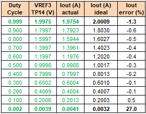
This graph displays the measured output current versus CHG ISET DAC at an input voltage of 400 Vdc. A PWM signal is provided at J8 with a frequency of 100 kHz, an amplitude of 2.5 V, and a duty cycle varying between 0% and 100%. A constant resistance mode load of 200 Ω is used and VOUT is allowed to vary with the current control.
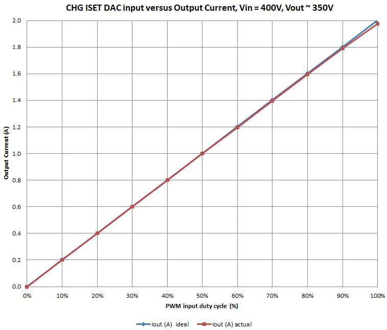
GUID-20210611-CA0I-2QJ9-0XTW-3SKS6GFRGTWW-low.png Figure 3-7 CHG ISET DAC Accuracy Curve
GUID-20210614-CA0I-020D-SK9B-QMPBJDRZ8D8Q-low.png Figure 3-8 CHG ISET DAC Accuracy Table