TIDT244 July   2021


  1. 1Description
  2. 2Test Prerequisites
    1. 2.1 Voltage and Current Requirements
    2. 2.2 Required Equipment
  3. 3Testing and Results
    1. 3.1 Thermal Images
    2. 3.2 Efficiency and Power Dissipation Graph
    3. 3.3 Efficiency and Power Dissipation Data
    4. 3.4 Current Regulation
    5. 3.5 Voltage Regulation
  4. 4Waveforms
    1. 4.1 Start-up
    2. 4.2 Switch Node
    3. 4.3 Output Voltage Ripple
    4. 4.4 Current Loop to Voltage Loop Transition
    5. 4.5 Voltage Loop to Current Loop Transition
    6. 4.6 Bias Voltage Start-up
    7. 4.7 Bias Voltage Switch Nodes
    8. 4.8 Output Current Sense Signal

Thermal Images

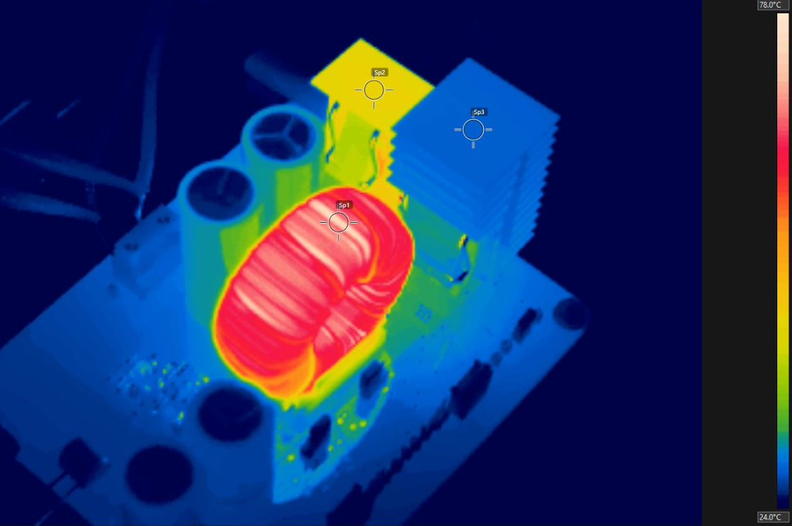
The following images show the operating temperature of the board with 400-Vdc input and 400 V at 2-A output at room temperature with approximately 200 LFM to 400 LFM of air flow.
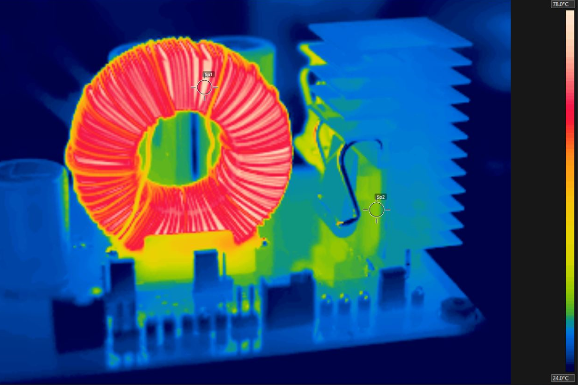
GUID-20210616-CA0I-KWZJ-PRLF-KVBFHN77ND76-low.pngFigure 3-1 Front Thermal Image
Measurement LocationTemperature (°C)
Sp175.6
Sp237.1
GUID-20210616-CA0I-Z1DQ-FNZ1-JLBGXMH30KS5-low.pngFigure 3-2 Top Thermal Image
Measurement LocationTemperature (°C)
Sp175.9
Sp2

47.6

Sp329.2