SBAA548A April   2022  – May 2022 ADS8588S , ADS8681 , ADS8686S , ADS8688 , ADS8688A


  1.   Abstract
  2.   Trademarks
  3. 1Introduction
  4. 2Circuit Design and Test System
    1. 2.1 Design Description
      1. 2.1.1 Input Protection
      2. 2.1.2 Power Supply Design and Protection
      3. 2.1.3 Digital Isolation Design
      4. 2.1.4 Component Selection and Layout Considerations
    2. 2.2 Test System
      1. 2.2.1 Reference
    3. 2.3 Standards and Test Criteria
  5. 3Test Details and Results
    1. 3.1 Electrical Fast Transients (EFT)
    2. 3.2 Electrostatic Discharge (ESD)
    3. 3.3 Surge Immunity (SI)
    4. 3.4 Conducted Immunity (CI)
    5. 3.5 Radiated Immunity (RI)
    6. 3.6 Radiated Emissions (RE)
      1.      20
  6. 4Schematics
  7. 5PCB Layouts
  8. 6Bill of Materials
  9. 7Acknowledgments
  10. 8References
  11. 9Revision History

Schematics

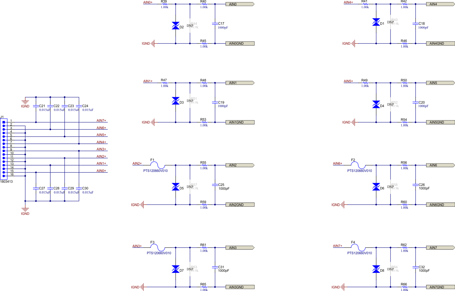
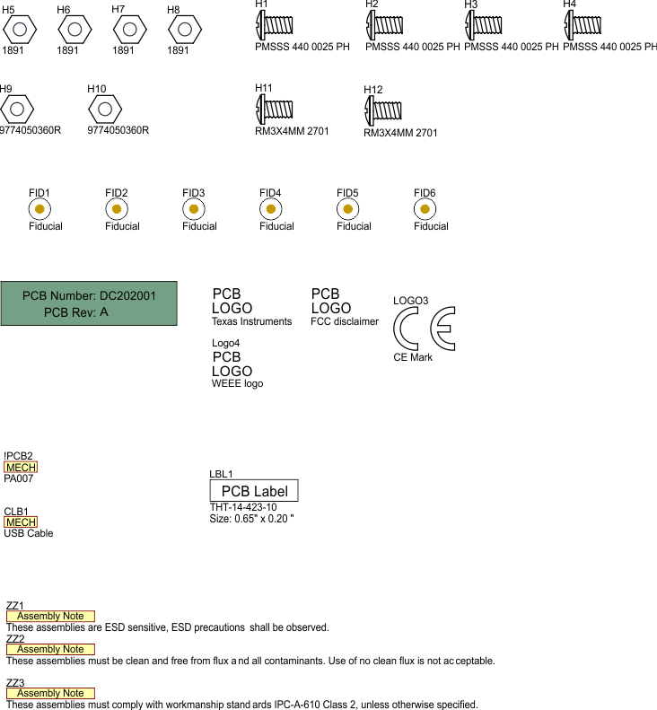
Figure 4-1 through Figure 4-6 show the schematics.
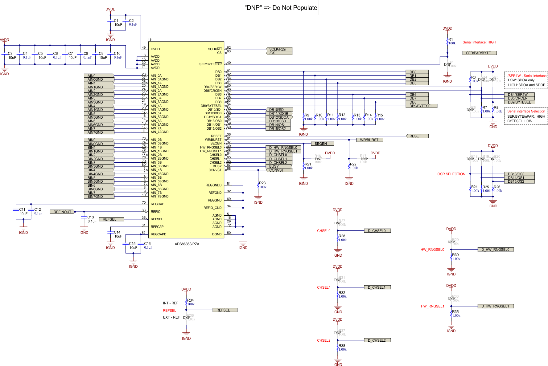
GUID-20220322-SS0I-GCXT-071S-NHNMTBPWLXHM-low.gif Figure 4-1 Schematic – ADC
GUID-20220322-SS0I-9JJX-GBJ1-6JTQHMGKNQNQ-low.gif Figure 4-2 Schematic – Input of ADC - A
GUID-20220322-SS0I-1NM7-J1GV-4ZLH8QGJ4G22-low.gif Figure 4-3 Schematic – Input of ADC - B
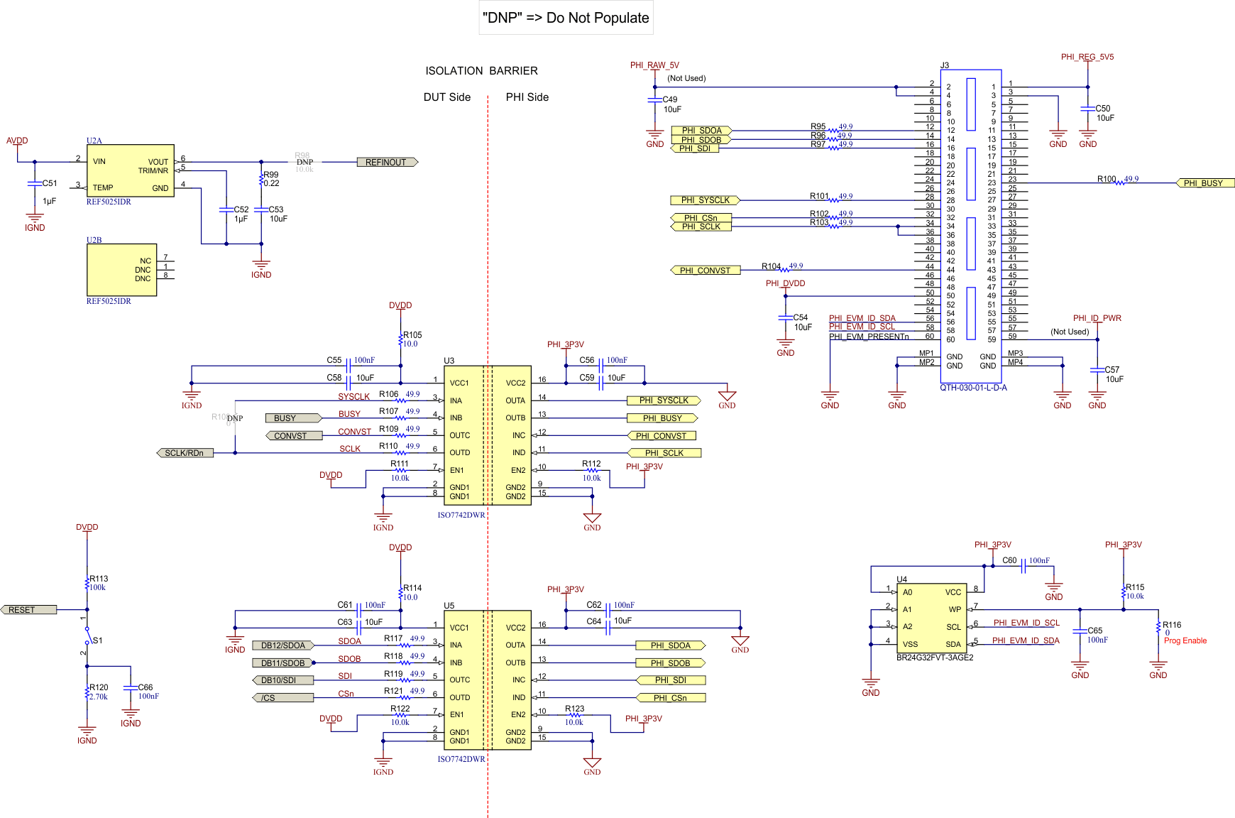
GUID-20220322-SS0I-8CHT-PWQS-0WD0MM2XXWDW-low.gif Figure 4-4 Schematic – Digital Isolation
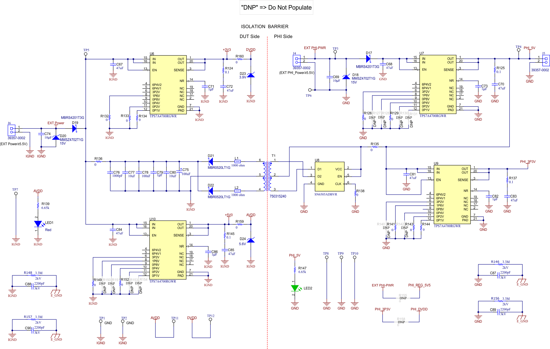
GUID-20220322-SS0I-4BKN-WBG6-5KZJMP2XBNCC-low.gif Figure 4-5 Schematic – Power Supply
GUID-20220322-SS0I-LKDT-NVNS-4G5Z1GCDDR78-low.gif Figure 4-6 Schematic – Hardware