SCDA008C June   2021  – November 2021 CD4052B , TS3A225E , TS3A44159


  1.   Trademarks
  2. 1Introduction
  3. 2Semiconductor Switches
    1. 2.1 NMOS Switch
    2. 2.2 PMOS Switch
  4. 3Basic Signal-Switch Structures
    1. 3.1 NMOS Series Switch
    2. 3.2 NMOS/PMOS Parallel Switch
    3. 3.3 NMOS Series Switch with the Charge Pump
  5. 4Key Concerns in Digital-Switch Applications
    1. 4.1  Power and Control Voltage Requirements
    2. 4.2  Rail-to-Rail Operation
    3. 4.3  Undershoot
    4. 4.4  ron
    5. 4.5  Cio(off)
    6. 4.6  Cio(on)
    7. 4.7  Ci (Control Input Capacitance)
    8. 4.8  Leakage Current
    9. 4.9  Enable and Disable Delays and Propagation Delay
    10. 4.10 Partial Power Down
    11. 4.11 Voltage Translation
  6. 5Signal Switch Families
    1. 5.1 CBT-C Family
      1. 5.1.1 Characteristics of CBT-C Family
        1. 5.1.1.1 VOvs VI
        2. 5.1.1.2 ron vs VI
        3. 5.1.1.3 Undershoot Protection
      2. 5.1.2 Application of CBT-C Family
        1. 5.1.2.1 Bus Isolation
    2. 5.2 CBTLV Family
      1. 5.2.1 Characteristics of the CBTLV Family
    3. 5.3 CB3Q Family
      1. 5.3.1 Characteristics of the CB3Q Family
        1. 5.3.1.1 VOvs VI
        2. 5.3.1.2 ron vs VI
        3. 5.3.1.3 Operation at High Frequency
        4. 5.3.1.4 Output Skew
        5. 5.3.1.5 Frequency Response
        6. 5.3.1.6 Adjacent Channel Crosstalk
      2. 5.3.2 Application of the CB3Q Family
        1. 5.3.2.1 Multiplexer in USB Applications
    4. 5.4 CB3T Family
      1. 5.4.1 Characteristics of the CB3T Family
        1. 5.4.1.1 VO vs VI
        2. 5.4.1.2 ron vs VI
        3. 5.4.1.3 Operation at High Frequency
      2. 5.4.2 Application of the CB3T Family
        1. 5.4.2.1 Voltage Translation for an External Monitor Terminal in a Notebook PC
  7. 6Applications
    1. 6.1 Multiplexing USB Peripherals
    2. 6.2 Multiplexing Ethernet
    3. 6.3 Notebook Docking Station
  8. 7Conclusion
  9. 8References
  10. 9Revision History
  11.   A Test Measurement Circuits
    1.     A.1 Measurement Setup for ron
    2.     A.2 Measurement Setup for VO vs VI Characteristics
    3.     A.3 Voltage-Time Waveform Measurement (Switch On)
    4.     A.4 Voltage-Time Waveform Measurement (Switch Off)
    5.     A.5 Output-Skew Measurement
    6.     A.6 Simulation Setup for Undershoot Measurement
    7.     A.7 Laboratory Setup for Attenuation Measurement
    8.     A.8 Laboratory Setup for Off Isolation Measurement
    9.     A.9 Laboratory Setup for Crosstalk Measurement

Operation at High Frequency

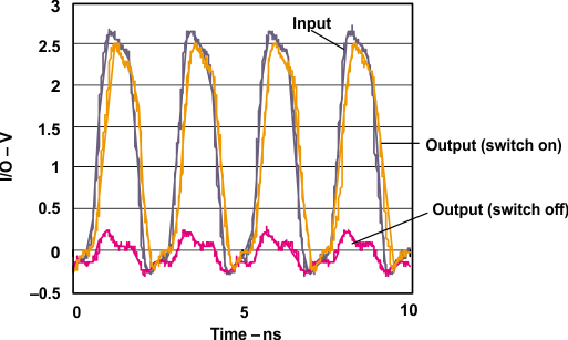
Low input and output capacitance, low ron, and low feed-through capacitance makes the CB3Q devices suitable for high-speed applications. Maximum frequency of operation depends on input voltage range, type of load, edge rate, type of package, off-isolation, crosstalk requirement, and so forth At high frequencies, off-isolation and crosstalk also increase, which limits the maximum frequency of operation. Figure 5-14 shows the input and output voltage waveforms at a frequency of 420 MHz, with a 500-Ω and 3-pF load. From Figure 5-14, it is clear that the switch, when on, allows high-frequency signals to pass without distortion. Also, the switch provides very good isolation between the input and output when it is turned off or disabled.
GUID-930C0461-1B79-4375-A528-B2883ACCA296-low.gifFigure 5-14 Input and Output Voltage Waveforms for the CB3Q3306A at 420 MHz (VCC = 3.3 V)