SCDA008C June 2021 – November 2021 CD4052B , TS3A225E , TS3A44159
- Trademarks
- 1Introduction
- 2Semiconductor Switches
- 3Basic Signal-Switch Structures
- 4Key Concerns in Digital-Switch Applications
- 5Signal Switch Families
- 6Applications
- 7Conclusion
- 8References
- 9Revision History
-
A Test
Measurement Circuits
- A.1 Measurement Setup for ron
- A.2 Measurement Setup for VO vs VI Characteristics
- A.3 Voltage-Time Waveform Measurement (Switch On)
- A.4 Voltage-Time Waveform Measurement (Switch Off)
- A.5 Output-Skew Measurement
- A.6 Simulation Setup for Undershoot Measurement
- A.7 Laboratory Setup for Attenuation Measurement
- A.8 Laboratory Setup for Off Isolation Measurement
- A.9 Laboratory Setup for Crosstalk Measurement
4.3 Undershoot
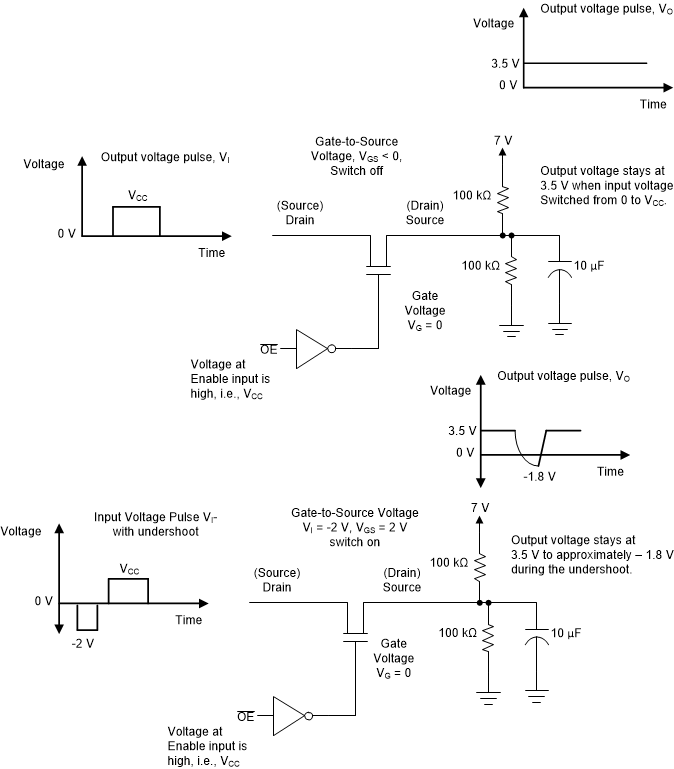
Undershoot is a typical phenomenon in high-speed applications where impedance mismatches cause excessive ringing in the system. This poses a serious problem to bus switches that are turned off and attempt to isolate different buses. In this state, the gate voltage of the n-channel pass transistors are at ground potential, but a negative voltage on either I/O port with a magnitude greater than the NMOS VT will cause the switch to conduct and no longer isolate the buses. Therefore, undershoots with a large magnitude and long duration result in data corruption, if no undershoot protection circuitry is included in the signal-switch design. The schematics in Figure 4-3 demonstrate the phenomenon of undershoots. For normal input voltages ranging from 0 V to VCC, the switch is in the high-impedance state and the output bus is isolated from the input bus. The undershoot produces a glitch at the isolated bus, as shown in Figure 4-3.
 Figure 4-3 Undershoot in NMOS Series-Switch Devices When Disabled
There are two solutions to prevent the NMOS from turning on during the undershoot even while disabled:
- Capture or clamp the input undershoot energy. In this method, a clamp circuit is connected to ground or VCC. This clamp circuit prevents the NMOS from turning on while an undershoot event occurs.
- Schottky Clamp. In this method, a Schottky diode is connected from the I/O port of the switch to ground. When the voltage at the I/O port goes below ground, the diode is forward biased and clamps the source or drain voltage, keeping the input and output isolated. An example of this type of device is the CBTS bus switch provided by TI.
- Active clamp to VCC. In this method, an active clamp circuit is connected to VCC, which tries to counteract the undershoot voltage by pulling the input voltage to VCC. An example of this type of device is the CBTK bus switch provided by TI.
- Force the gate voltage of the NMOS to track the negative input voltage. TI’s new CBT-C family uses this method to prevent undershoot. This method of protection is described later in this application report.