SCDA008C June 2021 – November 2021 CD4052B , TS3A225E , TS3A44159
- Trademarks
- 1Introduction
- 2Semiconductor Switches
- 3Basic Signal-Switch Structures
- 4Key Concerns in Digital-Switch Applications
- 5Signal Switch Families
- 6Applications
- 7Conclusion
- 8References
- 9Revision History
-
A Test
Measurement Circuits
- A.1 Measurement Setup for ron
- A.2 Measurement Setup for VO vs VI Characteristics
- A.3 Voltage-Time Waveform Measurement (Switch On)
- A.4 Voltage-Time Waveform Measurement (Switch Off)
- A.5 Output-Skew Measurement
- A.6 Simulation Setup for Undershoot Measurement
- A.7 Laboratory Setup for Attenuation Measurement
- A.8 Laboratory Setup for Off Isolation Measurement
- A.9 Laboratory Setup for Crosstalk Measurement
5.4 CB3T Family
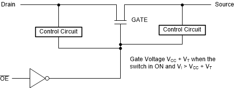
The CB3T (Cross-Bar Translating) family is a voltage-translation bus-switch family. This family can operate with a power-supply voltage range of 2.3 V to 3.6 V. When VCC = 3.3 V, the device can translate from a 5-V input to a 3.3-V output. In addition, when VCC = 2.3 V the device can translate from 5-V or 3.3-V inputs to a 2.3-V output. The CB3T family can be used for voltage translation at moderately high frequencies. Figure 5-22 shows the simplified structure of the CB3T3306.
 Figure 5-22 Simplified Structure of the CBT3306
When the switch is on, the voltage at the gate of the NMOS pass transistor in the CB3T3306 is biased at VCC + VT, where VT is the threshold voltage of the NMOS. When input voltage starts to rise from low to high, the output follows the input voltage. As the input voltage reaches about one-half of VCC, the control circuit senses this voltage and pulls the output voltage close to the VCC level and keeps the voltage constant as the input voltage increases. When the input reaches VCC + VT, the output voltage again increases to VCC and remains nearly flat, as the input voltage continues to rise. Input voltages at which these transitions occur depend on the output current, power supply, temperature, and transistor characteristics. The level of output high voltage (VOH) also depends on the output current.