SCDA008C June 2021 – November 2021 CD4052B , TS3A225E , TS3A44159
- Trademarks
- 1Introduction
- 2Semiconductor Switches
- 3Basic Signal-Switch Structures
- 4Key Concerns in Digital-Switch Applications
- 5Signal Switch Families
- 6Applications
- 7Conclusion
- 8References
- 9Revision History
-
A Test
Measurement Circuits
- A.1 Measurement Setup for ron
- A.2 Measurement Setup for VO vs VI Characteristics
- A.3 Voltage-Time Waveform Measurement (Switch On)
- A.4 Voltage-Time Waveform Measurement (Switch Off)
- A.5 Output-Skew Measurement
- A.6 Simulation Setup for Undershoot Measurement
- A.7 Laboratory Setup for Attenuation Measurement
- A.8 Laboratory Setup for Off Isolation Measurement
- A.9 Laboratory Setup for Crosstalk Measurement
5.3.2.1 Multiplexer in USB Applications
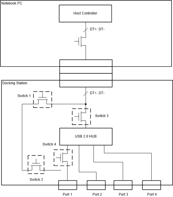
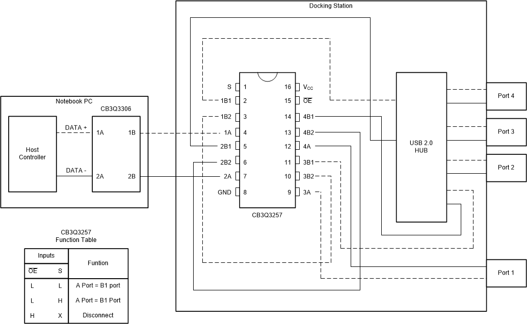
Figure 5-20 shows a USB 2.0 application in which a bus-switch device can be used. The first switch in a notebook PC is used to isolate between a notebook PC and the docking station. The switches on the docking station are used as a multiplexer to provide two different paths for the DATA+ and DATA– signals. If the operating system is Windows 95, the USB 2.0 hub is not supported. Switches 1 and 2 are on, and the USB line is connected directly to Port 1. Figure 5-21 shows the use of a CB3Q3257 in this type of application.
 Figure 5-20 Multiplexing in a USB Application
 Figure 5-21 CB3Q3257 in a USB Application
DATA+ signal path is shown as a dotted line and the DATA– signal is shown as a solid line. The DATA+ signal goes to 1A. Depending on the select signal (S) levels, the output can be 1B1 or 1B2. When S is low, DATA+ from the host controller is connected to the port through the USB 2.0 hub (1A → 1B1 → USB 2.0 Hub → 3B1 → 3A → Port 1). When S is high, the DATA+ is connected to port 1 directly (1A → 1B2 → 3B2 → 3A). Similarly, DATA– uses the 2A, 2B1, 2B2 and 4A, 4B1, 4B2 switches for connecting to port 1.