SCDA008C June 2021 – November 2021 CD4052B , TS3A225E , TS3A44159
- Trademarks
- 1Introduction
- 2Semiconductor Switches
- 3Basic Signal-Switch Structures
- 4Key Concerns in Digital-Switch Applications
- 5Signal Switch Families
- 6Applications
- 7Conclusion
- 8References
- 9Revision History
-
A Test
Measurement Circuits
- A.1 Measurement Setup for ron
- A.2 Measurement Setup for VO vs VI Characteristics
- A.3 Voltage-Time Waveform Measurement (Switch On)
- A.4 Voltage-Time Waveform Measurement (Switch Off)
- A.5 Output-Skew Measurement
- A.6 Simulation Setup for Undershoot Measurement
- A.7 Laboratory Setup for Attenuation Measurement
- A.8 Laboratory Setup for Off Isolation Measurement
- A.9 Laboratory Setup for Crosstalk Measurement
3.3 NMOS Series Switch with the Charge Pump
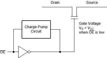
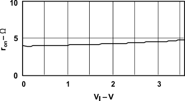
Although, in an NMOS/PMOS parallel switch, source-to-drain resistance is lower than in an NMOS series switch, the PMOS adds capacitance, which is undesirable for some applications. To solve this problem, another type of switch structure is used that involves a charge-pump circuit in the NMOS series switch. The charge-pump circuit generates a voltage at the gate of the NMOS that is 2 V to 3 V higher than VCC. As a result, when the input reaches the VCC level, the switch still is on and the output voltage is equal to the input voltage over the 0 V to VCC input voltage range. The disadvantage of implementing a charge-pump circuit in the NMOS series switch is the additional power consumption because of the charge-pump circuit. Figure 3-5 shows a simple schematic of an NMOS series switch with the charge pump, and Figure 3-6 shows the ron versus VI characteristic.
 Figure 3-5 Basic Structure of an NMOS Series Switch with the Charge Pump
 Figure 3-6 ron vs VI in an NMOS Series Switch with the Charge Pump (VCC = 3.6 V)