SCDA008C June 2021 – November 2021 CD4052B , TS3A225E , TS3A44159
- Trademarks
- 1Introduction
- 2Semiconductor Switches
- 3Basic Signal-Switch Structures
- 4Key Concerns in Digital-Switch Applications
- 5Signal Switch Families
- 6Applications
- 7Conclusion
- 8References
- 9Revision History
-
A Test
Measurement Circuits
- A.1 Measurement Setup for ron
- A.2 Measurement Setup for VO vs VI Characteristics
- A.3 Voltage-Time Waveform Measurement (Switch On)
- A.4 Voltage-Time Waveform Measurement (Switch Off)
- A.5 Output-Skew Measurement
- A.6 Simulation Setup for Undershoot Measurement
- A.7 Laboratory Setup for Attenuation Measurement
- A.8 Laboratory Setup for Off Isolation Measurement
- A.9 Laboratory Setup for Crosstalk Measurement
4.2 Rail-to-Rail Operation
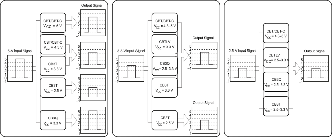
Rail-to-rail operation describes the behavior where a signal switch passes signals that range between the most positive and most negative supply rails. Switches with rail-to-rail operation will pass signals with little to no voltage drop when the signal falls at or between the voltage rails. Figure 4-2 shows the behavior of different switches operating at different signal and rail levels.
 Figure 4-2 Signal Levels Through Digital Switches
Digital signals between communicating devices usually must meet some minimum voltage level to be registered as a high signal. All devices along a signal path, including a digital switch, should be considered when determining the efficacy of a design. Reduced high-level voltages from non-rail-to-rail switches should be considered, and designs should ensure that appropriate signal levels will be attained. Using rail-to-rail switches minimizes or removes risk from this phenomenon. Certain switches, like the CB3T and CB3Q families, allow I/O voltages beyond the supply, allowing designers increased opportunity for effective implementation and design.