SLAA834B May 2018 – August 2021 MSP430FR2000 , MSP430FR2032 , MSP430FR2033 , MSP430FR2100 , MSP430FR2110 , MSP430FR2111 , MSP430FR2153 , MSP430FR2155 , MSP430FR2310 , MSP430FR2311 , MSP430FR2353 , MSP430FR2355 , MSP430FR2422 , MSP430FR2433 , MSP430FR2475 , MSP430FR2476 , MSP430FR2512 , MSP430FR2522 , MSP430FR2532 , MSP430FR2533 , MSP430FR2632 , MSP430FR2633 , MSP430FR2672 , MSP430FR2673 , MSP430FR2675 , MSP430FR2676 , MSP430FR4131 , MSP430FR4132 , MSP430FR4133 , MSP430FR5720 , MSP430FR5721 , MSP430FR5722 , MSP430FR5723 , MSP430FR5724 , MSP430FR5725 , MSP430FR5726 , MSP430FR5727 , MSP430FR5728 , MSP430FR5729 , MSP430FR5730 , MSP430FR5731 , MSP430FR5732 , MSP430FR5733 , MSP430FR5734 , MSP430FR5735 , MSP430FR5736 , MSP430FR5737 , MSP430FR5738 , MSP430FR5739 , MSP430FR5847 , MSP430FR58471 , MSP430FR5848 , MSP430FR5849 , MSP430FR5857 , MSP430FR5858 , MSP430FR5859 , MSP430FR5867 , MSP430FR58671 , MSP430FR5868 , MSP430FR5869 , MSP430FR5870 , MSP430FR5872 , MSP430FR58721 , MSP430FR5887 , MSP430FR5888 , MSP430FR5889 , MSP430FR58891 , MSP430FR5922 , MSP430FR59221 , MSP430FR5947 , MSP430FR59471 , MSP430FR5948 , MSP430FR5949 , MSP430FR5957 , MSP430FR5958 , MSP430FR5959 , MSP430FR5962 , MSP430FR5964 , MSP430FR5967 , MSP430FR5968 , MSP430FR5969 , MSP430FR59691 , MSP430FR5970 , MSP430FR5972 , MSP430FR59721 , MSP430FR5986 , MSP430FR5987 , MSP430FR5988 , MSP430FR5989 , MSP430FR59891 , MSP430FR5992 , MSP430FR5994 , MSP430FR59941
- Trademarks
- 1 Introduction
- 2 Configuration of MSP430FR4xx and MSP430FR2xx Devices
- 3 In-System Programming of Nonvolatile Memory
- 4 Hardware Migration Considerations
- 5 Device Calibration Information
- 6 Important Device Specifications
- 7 Core Architecture Considerations
-
8 Peripheral Considerations
- 8.1 Overview of the Peripherals on the FR4xx and FR59xx Families
- 8.2 Ports
- 8.3 Communication Modules
- 8.4 Timer and IR Modulation Logic
- 8.5 Backup Memory
- 8.6 RTC Counter
- 8.7 LCD
- 8.8 Interrupt Compare Controller (ICC)
- 8.9 Analog-to-Digital Converters
- 8.10 Enhanced Comparator (eCOMP)
- 8.11 Operational Amplifiers
- 8.12 Smart Analog Combo (SAC)
- 9 ROM Libraries
- 10Conclusion
- 11References
- 12Revision History
7.1.1 Core LDO and LPM3.5 LDO
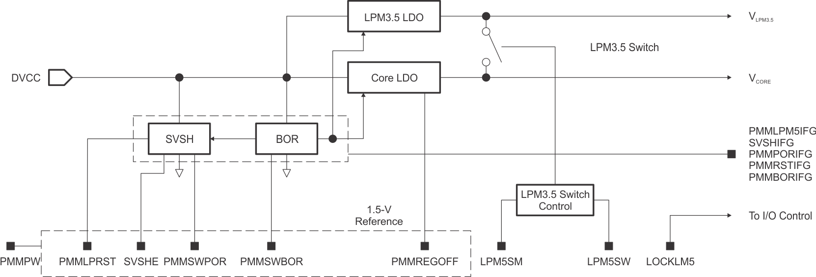
The FR4xx family uses a single voltage supply. However unlike FR59xx, there are no AVCC and AVSS pins, only DVCC and DVSS. The external voltage supply on the DVCC pin is fed to an internal low-dropout voltage regulator (LDO) (see Figure 7-1).
 Figure 7-1 FR4xx PMM Block Diagram
The PMM manages all functions related to the core voltage and its supervision. Its primary functions are, first, to generate a supply voltage for the core logic and, second, to provide several mechanisms for the supervision of both the voltage supplied to the device (DVCC) and the voltage generated for the core (VCORE).
Using the PMM is especially advantageous as it allows the core to operate at a lower voltage, which brings significant power savings. It also ensures that the core receives a stable and regulated voltage over a wide supply range.
There is a second LDO integrated in FR4xx, the LPM3.5 LDO. This LDO supplies the current for the LPM3.5 power domain logic, which contains the RTC and LCD modules (only the MSP430FR4xx MCUs have the LCD module). In LPMx.5 low-power modes, the Core LDO is turned off. When entering LPM3.5, the LPM3.5 switch is turned off to save power consumption. When exiting LPM3.5 power mode, the LPM3.5 switch is turned on so that the core LDO can supply power to the LPM3.5 domain logic to support high-frequency operation (see Figure 7-1).