SLOA011B January 2018 – July 2021 LF347 , LF353 , LM348 , MC1458 , TL022 , TL061 , TL062 , TL071 , TL072 , UA741
- 1Introduction
- 2Non-Inverting Amplifier
- 3Inverting Amplifier
- 4Simplified Op Amp Circuit Diagram
-
5Op Amp Specifications
- 5.1 Absolute Maximum Ratings and Recommended Operating Condition
- 5.2 Input Offset Voltage
- 5.3 Input Current
- 5.4 Input Common Mode Voltage Range
- 5.5 Differential Input Voltage Range
- 5.6 Maximum Output Voltage Swing
- 5.7 Large Signal Differential Voltage Amplification
- 5.8 Input Parasitic Elements
- 5.9 Output Impedance
- 5.10 Common-Mode Rejection Ratio
- 5.11 Supply Voltage Rejection Ratio
- 5.12 Supply Current
- 5.13 Slew Rate at Unity Gain
- 5.14 Equivalent Input Noise
- 5.15 Total Harmonic Distortion Plus Noise
- 5.16 Unity-Gain Bandwidth and Phase Margin
- 5.17 Settling Time
- 6References
- 7Glossary
- 8Revision History
3 Inverting Amplifier
Figure 3-1 shows another useful basic op amp circuit, the inverting amplifier. The triangular gain block symbol is again used to represent an ideal op amp. The input terminal, + (Vp), is called the non-inverting input, whereas – (Vn) marks the inverting input. It is similar to the non-inverting circuit shown in Figure 2-1 except that now the signal is applied to the inverting terminal via R1 and the non-inverting terminal is grounded.
 Figure 3-1 Inverting Amplifier
To understand this circuit, we must derive a relationship between the input voltage, Vi and the output voltage, Vo.
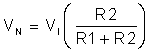
Since Vp is tied to ground,
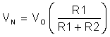
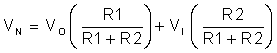
Remembering that there is no current into the input, the voltage at Vn can be found using superposition. First let Vo = 0,
Next let Vi = 0,
Combining
Remembering equation Equation 14, Vo = aVd = a(Vp - Vn), substituting and rearranging,
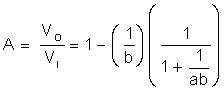
where

Again we have an amplifier circuit. Because b ≤ 1, the closed loop gain, A, is negative, and the polarity of Vo will be opposite to Vi. Therefore, this is an inverting amplifier.