SLOA011B January 2018 – July 2021 LF347 , LF353 , LM348 , MC1458 , TL022 , TL061 , TL062 , TL071 , TL072 , UA741
- 1Introduction
- 2Non-Inverting Amplifier
- 3Inverting Amplifier
- 4Simplified Op Amp Circuit Diagram
-
5Op Amp Specifications
- 5.1 Absolute Maximum Ratings and Recommended Operating Condition
- 5.2 Input Offset Voltage
- 5.3 Input Current
- 5.4 Input Common Mode Voltage Range
- 5.5 Differential Input Voltage Range
- 5.6 Maximum Output Voltage Swing
- 5.7 Large Signal Differential Voltage Amplification
- 5.8 Input Parasitic Elements
- 5.9 Output Impedance
- 5.10 Common-Mode Rejection Ratio
- 5.11 Supply Voltage Rejection Ratio
- 5.12 Supply Current
- 5.13 Slew Rate at Unity Gain
- 5.14 Equivalent Input Noise
- 5.15 Total Harmonic Distortion Plus Noise
- 5.16 Unity-Gain Bandwidth and Phase Margin
- 5.17 Settling Time
- 6References
- 7Glossary
- 8Revision History
5.7 Large Signal Differential Voltage Amplification
Large signal differential voltage amplification, AVD, is the ratio of the output voltage change to the input differential voltage change, while holding VCM constant. This parameter is closely related to the open loop gain. The difference is that it is measured with an output load and therefore takes into account loading effects.
The DC value of AVD is published in the data sheet, but AVD is frequency dependent. Figure 5-12 shows a typical graph of AVD vs. frequency.
AVD is a design issue when precise gain is required. Consider equation Equation 16, where the loop gain of the non-inverting amplifier is given by:
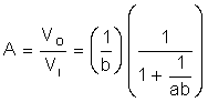
where,

It is desired to control the gain of the circuit by selecting the appropriate resistors. The term 1/ab in the equation is seen as an error term. Unless a, or AVD, is large in comparison with 1/b, it will have an undesired effect on the gain of the circuit.