SLOA011B January 2018 – July 2021 LF347 , LF353 , LM348 , MC1458 , TL022 , TL061 , TL062 , TL071 , TL072 , UA741
- 1Introduction
- 2Non-Inverting Amplifier
- 3Inverting Amplifier
- 4Simplified Op Amp Circuit Diagram
-
5Op Amp Specifications
- 5.1 Absolute Maximum Ratings and Recommended Operating Condition
- 5.2 Input Offset Voltage
- 5.3 Input Current
- 5.4 Input Common Mode Voltage Range
- 5.5 Differential Input Voltage Range
- 5.6 Maximum Output Voltage Swing
- 5.7 Large Signal Differential Voltage Amplification
- 5.8 Input Parasitic Elements
- 5.9 Output Impedance
- 5.10 Common-Mode Rejection Ratio
- 5.11 Supply Voltage Rejection Ratio
- 5.12 Supply Current
- 5.13 Slew Rate at Unity Gain
- 5.14 Equivalent Input Noise
- 5.15 Total Harmonic Distortion Plus Noise
- 5.16 Unity-Gain Bandwidth and Phase Margin
- 5.17 Settling Time
- 6References
- 7Glossary
- 8Revision History
5.16 Unity-Gain Bandwidth and Phase Margin
There are five parameters that relate to the frequency characteristics of the op amp that you will encounter in Texas Instruments’ data sheets:
- Unity-gain bandwidth (B1)
- Gain bandwidth product (GBW)
- Phase margin at unity gain (φm)
- Gain margin
- Maximum output-swing bandwidth (BOM)
Unity-gain bandwidth (B1) and gain bandwidth product (GBW) are similar. B1 specifies the frequency at which AVD of the op amp is 1:
GBW specifies the gain-bandwidth product of the op amp in an open loop configuration and the output loaded:
Phase margin at unity gain (fm) is the difference between the amount of phase shift a signal experiences through the op amp at unity gain and 180°:
Gain margin is the difference between unity gain and the gain at 180° phase shift:
Maximum output-swing bandwidth (BOM) specifies the bandwidth over which the output is above a specified value:
The limiting factor for BOM is slew rate. As the frequency gets higher and higher the output becomes slew rate limited and can not respond quickly enough to maintain the specified output voltage swing.
To make the op amp stable, capacitor, CC, is purposely fabricated on chip in the second stage (see Figure 4-1). This type of frequency compensation is termed dominant pole compensation. The idea is to cause the open-loop gain of the op amp to role off to unity before the output phase shifts by 180°. Remember that Figure 4-1 is very simplified: there are other frequency shaping elements within a real op amp. Figure 5-11 shows a typical gain vs. frequency plot for an internally compensated op amp as normally presented in a Texas Instruments data sheet. Figure 5-12 contains the same information except the phase axis is shifted for clarity.
As noted earlier, it can be seen that AVD falls off with frequency. AVD (and thus B1 or GBW) is a design issue when precise gain is required of a specific frequency band. Consider equation Equation 16, where the loop gain of the non-inverting amplifier is given by:
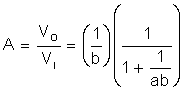
It is desired to control the gain of the circuit by selecting the appropriate resistors. The term 1/ab in the equation is seen as an error term. Unless a, or AVD, is large for all frequencies of interest in comparison with 1/b, a will have an effect on the gain of the circuit, which is undesired.
Phase margin (φm) and gain margin are different ways of specifying the stability of the circuit. Since rail-to-rail output op amps have higher output impedance, a significant phase shift is seen when driving capacitive loads. This extra phase shift erodes the phase margin, and for this reason most CMOS op amps with rail-to-rail outputs have limited ability to drive capacitive loads.
 Figure 5-11 Typical Large-Signal Differential Voltage Amplification and Phase Shift vs. Frequency
 Figure 5-12 Easier to Read Graph of Voltage Amplification and Phase Shift vs. Frequency